
This document describes high-speed hex buffers with 3-state outputs. They can be organized as a single 6-bit or 2-bit/4-bit, with inverting or non-inverting data paths. The outputs can drive 15 TTL Unit Loads or 60 Low Power Schottky loads when the Enable is LOW. When the Output Enable is HIGH, the outputs are forced to a high impedance 'off' state. If the outputs of the 3-state devices are tied together, all but one device must be in the high impedance state to avoid high currents that would exceed the maximum ratings. Designers should ensure that Output Enable signals to 3-state devices whose outputs are tied together are designed so there is no overlap.
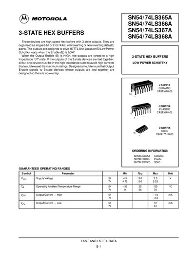
This document provides technical specifications and ordering information for the SN54/74LS365A, SN54/74LS366A, SN54/74LS367A, and SN54/74LS368A devices. These are high-speed hex buffers featuring 3-state outputs designed to drive up to 15 TTL unit loads or 60 low-power Schottky loads when the enable input is LOW.
| Supply Voltage (Voc) | 4.5 V to 5.5 V (SN54); 4.75 V to 5.25 V (SN74) |
|---|---|
| Operating Temperature Range | -55°C to +125°C (SN54); 0°C to +70°C (SN74) |
| Output Current High | -1.0 mA (SN54); -2.6 mA (SN74) |
| Output Current Low | 12 mA (SN54); 24 mA (SN74) |
The maximum output current for low state in SN54 devices is 12 mA.
The guaranteed minimum input high voltage for all inputs is 2.0 V.