
The MC88915T Clock Driver utilizes phase-locked loop technology to lock its low skew outputs’ frequency and phase onto an input reference clock. It is designed to provide clock distribution for high-performance PCs and workstations. The PLL allows the high current, low skew outputs to lock onto a single clock input and distribute it with essentially zero delay to multiple components on a board. The PLL also allows the MC88915T to multiply a low-frequency input clock and distribute it locally at a higher (2X) system frequency. Multiple 88915s can lock onto a single reference clock, which is ideal for applications when a central system clock must be distributed synchronously to multiple boards.
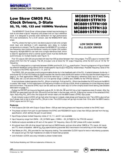
The MC88915T is a low skew CMOS Phase-Locked Loop (PLL) clock driver designed to distribute high-performance clocks for PCs and workstations. It utilizes phase-locked loop technology to lock its outputs' frequency and phase onto an input reference clock, providing essentially zero delay distribution to multiple components on a board.
The device features five 'Q' outputs with less than 500 ps skew between rising edges, along with additional outputs for inverted signals (Q5), doubled frequency (2X_Q), and halved frequency (Q/2). It supports input/output phase-locked frequency ratios of 1:2, 1:1, and 2:1. The chip includes a lock indicator output and test mode capabilities via the PLL_EN pin for low-frequency board testing.
| Output-Output Skew (Rising) | < 500 ps |
|---|---|
| Input Frequency Range | 5MHz — 2X_Q FMAX spec. |
| Output Drive Current | +36 mA |
| Operating Temperature Range | -40° C to +85° C |
The device provides five 'Q' outputs (Q0-Q4), plus additional outputs for inverted, doubled, and halved frequencies.
Pulling the PLL_EN pin low disables the VCO and puts the chip into a static 'test mode' for low frequency board testing.