
The CY7C1370CV25 and CY7C1372CV25 are 2.5V, 512K x 36 and 1M x 18 Synchronous pipelined burst SRAMs with No Bus Latency™ (NoBL) logic, respectively. They are designed to support unlimited true back-to-back Read/Write operations with no wait states. The CY7C1370CV25 and CY7C1372CV25 are equipped with the advanced (NoBL) logic required to enable consecutive Read/Write operations with data being transferred on every clock cycle. This feature dramatic
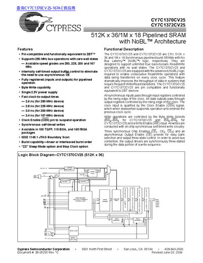
This document describes the CY7C1370CV25 (512K x 36) and CY7C1372CV25 (1M x 18) synchronous pipelined burst SRAMs. These devices feature Cypress Semiconductor's NoBL™ (No Bus Latency) logic, designed to support unlimited true back-to-back Read/Write operations with zero wait states at speeds up to 250 MHz.
The datasheet provides functional descriptions, pin configurations for various packages including TQFP, BGA, and fBGA, and detailed definitions for all input/output pins. It also includes a selection guide listing maximum access times and operating currents for different speed grades ranging from 167 to 250 MHz.
| Voltage Supply | 2.5V |
|---|---|
| Maximum Operating Frequency | 250 MHz |
| Clock-to-Output Time (250-MHz) | 2.6 ns |
These devices operate with a single 2.5V power supply.
The maximum operating current is 350 mA.