
XC6101~XC6107, XC6111~XC6117 series are groups of high-precision, low current consumption voltage detectors with manual reset input function and watchdog functions incorporating CMOS process technology.
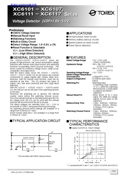
The document describes the XC6101~XC6107 and XC6111~XC6117 series as groups of high-precision, low current consumption voltage detectors utilizing CMOS technology. These ICs incorporate a reference voltage source, delay circuit, comparator, and output driver to provide reset signals with selectable release delays.
Key features include a detect voltage range from 1.6V to 5.0V in 100mV increments, six selectable watchdog timeout periods ranging from 6.25ms to 1.6s, and seven release delay times. The series offers two output configurations: VDFL (low when detected) and VDFH (high when detected), with options for CMOS or N-channel open drain outputs.
| Detect Voltage Range | 1.6V ~ 5.0V, +2% |
|---|---|
| Hysteresis Range (XC6101~XC6107) | VDF x 5%, TYP. |
| Hysteresis Range (XC6111~XC6117) | VDF x 0.1%, TYP. |
| Operating Voltage Range | 1.0V ~ 6.0V |
| Detect Voltage Temperature Characteristics | < 100ppm/°C (TYP) |
| Watchdog Timeout Periods | 6.25ms to 1.6sec |
| Release Delay Times | 3.13ms to 1.6sec |
| Output Configuration Options | N-channel open drain, CMOS |
The detect voltages are internally fixed from 1.6V to 5.0V in increments of 100mV.
Yes, for XC6101~XC6105 and XC6111~XC6115 series ICs, the WD pin can be left open if the watchdog function is not used.