
The SN74AUC2G125 is a dual bus buffer gate with 3-state outputs from TI. It has a working voltage range of 0.8V-2.7V, and a rated working voltage of 1.65V-1.95V. The device has low power consumption, low voltage, low output impedance, and high anti-interference.
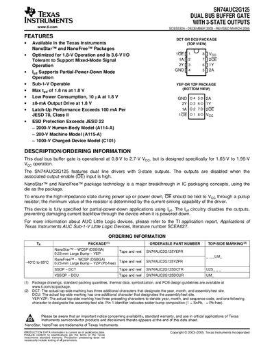
The document describes the SN74AUC2G125, a dual line driver featuring 3-state outputs optimized for sub-1-V operation between 0.8 V and 2.7 V supply voltages. The device is designed specifically for 1.65 V to 1.95 V operation and supports mixed-mode signal levels.
Key features include low power consumption, high latch-up performance exceeding 100 mA per JESD 78 Class II standards, and ESD protection exceeding JESD 22 specifications. The chip is available in NanoStar™, NanoFree™, DCT, DCU, YEP, and YZP packages.
| Supply Voltage Range | 0.8 V to 2.7 V |
|---|---|
| Optimized Supply Voltage | 1.65 V to 1.95 V |
| Max Output Drive Current (1.8 V) | +8 mA |
| Operating Temperature Range | -40°C to +85°C |
The device is operational at a supply voltage as low as 0.8 V.
All unused inputs must be held at VCC or GND to ensure proper device operation.
The outputs are disabled and enter a high-impedance state.