
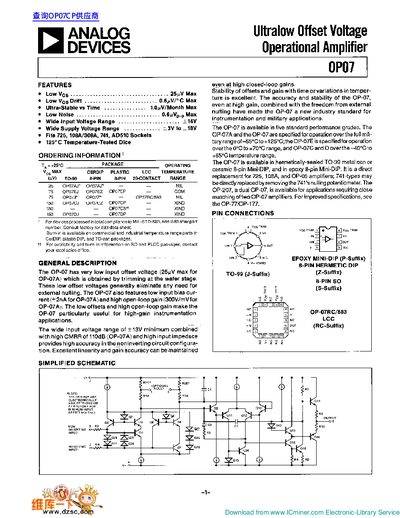
This document describes the OP07 series operational amplifiers, highlighting their ultralow input offset voltage (as low as 25 µV for the OP‑07A grade) and low input bias current. It covers the device’s wide supply voltage range, high open‑loop gain, and excellent temperature stability, making it suitable for high‑gain instrumentation and military applications.
The datasheet includes ordering information, pin‑out diagrams for J, P, and Z packages, absolute maximum ratings, detailed electrical characteristics, typical performance curves, and recommended application circuits such as precision thermocouple amplifiers and summing amplifiers.
| Input Offset Voltage | 25 µV (max, OP‑07A) |
|---|---|
| Power Supply Rejection Ratio | PSRR Vg = +3 V to +18 V |
| Supply Voltage Range | +3 V to +18 V |
| Closed‑Loop Bandwidth | 0.4 MHz‑0.6 MHz (typical) |
The OP‑07A grade has a maximum input offset voltage of 25 µV.
The device operates from +3 V up to +18 V.