
AD667 is a complete 12-bit D/A converter, featuring a dual-buffered latch and single-chip high stability buried Zener reference. The converter uses 12 precision high speed bipolar current steering switches and a laser trimmed thin-film resistor network to provide fast settling time and high accuracy. Microprocessor compatibility is achieved by the on-chip dual-buffered latch. The design of the input latch allows low input current and ensures linear dependence of output offset voltage on input bias current.
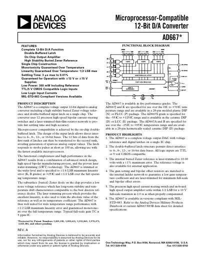
The AD667 is a complete 12‑bit voltage‑output DAC that integrates a high‑stability buried Zener reference, double‑buffered input latch and on‑chip output amplifier. It supports direct interfacing to 4‑, 8‑, 12‑ or 16‑bit buses and offers low‑power operation at 300 mW.
The document provides functional block diagrams, timing specifications, detailed electrical characteristics, pin‑out information, grounding recommendations and guidelines for optimizing settling time. Variants (J, K, A, B, S) are listed with their temperature ranges and package options.
| Settling Time (±0.01 % FS) | 2‑4 µs |
|---|---|
| Power Consumption | 300 mW |
| Supply Voltage | ±12 V or ±15 V |
| Output Current | ±5 mA |
It operates from ±12 V or ±15 V power supplies.
Settling time is between 2 µs and 4 µs depending on the feedback resistor value.