
MC74HC4051A/D, MC74HC4052A, MC74HC4053A are high performance silicon-gate CMOS devices featuring fast propagation delays, low ON resistances, and low OFF leakage currents. These analog multiplexers/demultiplexers control analog voltages that may vary across the complete power supply range (from VCC to VEE). The HC4051A, HC4052A and HC4053A are identical in pinout to the metal-gate MC14051AB, MC14052AB and MC14053AB. The Channel-Select inputs determine which one of the Analog Inputs/Outputs is to be connected, by means of an analog switch, to the Common Output/Input. When the Enable pin is HIGH, all analog switches are turned off. The Channel-Select and Enable inputs are compatible with standard CMOS outputs; with pullup resistors they are compatible with LSTTL outputs. These devices have been designed so that the ON resistance (Ron) is more linear over input voltage than Ron of metal-gate CMOS analog switches. For a multiplexer/demultiplexer with injection current protection, see HC4851A and HC4852A.
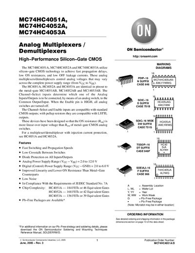
The MC74HC4051A, MC74HC4052A and MC74HC4053A are high‑performance silicon‑gate CMOS analog multiplexers/demultiplexers. They feature fast switching, low ON resistance, low crosstalk and diode protection on all inputs/outputs. The devices operate over a wide analog power‑supply range (2 V to 12 V) and a digital control range of 2 V to 6 V.
The data sheet provides detailed pin‑out diagrams, function tables, maximum ratings, recommended operating conditions, DC and AC characteristics, additional application notes, package dimensions and ordering information for each part number.
| Analog Power Supply Range (Vcc‑Veg) | 2.0 V to 12.0 V |
|---|---|
| Digital Control Power Supply Range (Vcc‑GND) | 2.0 V to 6.0 V |
| Maximum Propagation Delay (Channel‑Select to Analog Output) at Vcc=2.0 V | 270 ns (typical max) |
| Operating Temperature Range | -55 °C to +125 °C |
The analog power‑supply range is 2.0 V to 12.0 V.
The digital control voltage range is 2.0 V to 6.0 V.
The maximum propagation delay is 270 ns (typical) at a 2.0 V supply.
They operate from –55 °C up to +125 °C.