
AD5330/AD5331/AD5340/AD5341 are single voltage-output 8-/10-/12-bit DACs with a working voltage range of 2.5V to 5.5V and operating current of 115μA. They feature low power operation, double-buffered input logic, guaranteed monotonicity, etc.
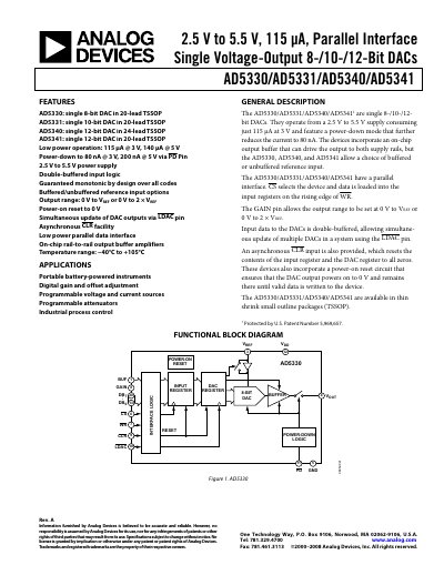
The AD5330, AD5331, AD5340 and AD5341 are single‑channel 8‑, 10‑ and 12‑bit digital‑to‑analog converters offered in thin‑shrink TSSOP packages. They operate from a 2.5 V to 5.5 V supply, consume low power (115 µA @ 3 V, 140 µA @ 5 V) and provide a parallel interface with double‑buffered input logic for simultaneous updates via the LDAC pin.
Key features include selectable output ranges (0 V‑VREF or 0 V‑2×VREF), power‑down current as low as 80 nA, rail‑to‑rail output buffers, guaranteed monotonicity, and an operating temperature range of –40 °C to +105 °C. The document details pin configurations, timing diagrams, absolute maximum ratings and typical application circuits.
| Supply Voltage (VDD) | 2.5 V to 5.5 V |
|---|---|
| Power Consumption (Normal Mode) | 115 µA @ 3 V, 140 µA @ 5 V |
| Power‑Down Current | 80 nA @ 3 V, 200 nA @ 5 V |
| Output Range | 0 V to VREF or 0 V to 2 × VREF |
| Operating Temperature Range | –40 °C to +105 °C |
| DC Output Impedance | 0.5 Ω |
| Short‑Circuit Current (VDD=5 V) | 25 mA |
They operate from 2.5 V to 5.5 V.
The power‑down current is 80 nA at 3 V and 200 nA at 5 V.
The devices are rated from –40 °C to +105 °C.