
AD5303/AD5313/AD5323 are dual rail-to-rail voltage output 8-bit/10-bit/12-bit DACs. They feature a voltage supply range of 2.5V to 5.5V, a current consumption of 230μA, and dual-buffered input logic with a low power serial interface.
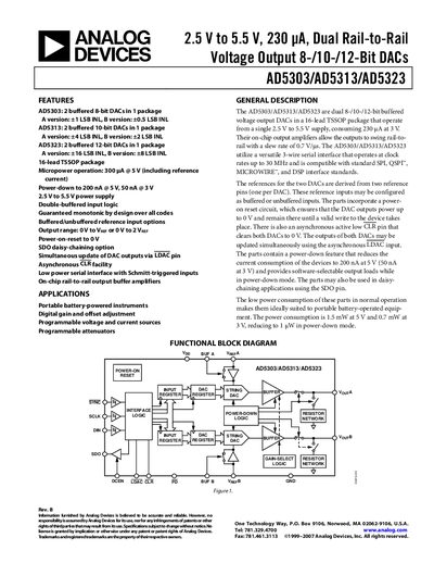
The AD5303, AD5313 and AD5323 are dual buffered DACs offered in a 16‑lead TSSOP package. They operate from a single 2.5 V to 5.5 V supply and provide rail‑to‑rail output with a slew rate of 0.7 V/µs. The devices support a versatile 3‑wire serial interface compatible with SPI, QSPI™, MICROWIRE™ and DSP standards, and include options for buffered or unbuffered reference inputs, power‑down mode, and daisy‑chain operation.
The datasheet details electrical specifications such as resolution (8, 10 or 12 bits), supply current (230 µA at 3 V), power‑down current (200 nA @ 5 V, 50 nA @ 3 V), output voltage range (0 V to VREF or 0 V to 2 VREF), output impedance (0.5 Ω), and timing parameters for the serial interface. Pin functions, absolute maximum ratings, and ordering information are also provided.
| Supply voltage range | 2.5 V to 5.5 V |
|---|---|
| Normal mode supply current | 230 µA @ 3 V |
| Power‑down current | 200 nA @ 5 V, 50 nA @ 3 V |
| Output voltage range | 0 V to VREF or 0 V to 2 VREF |
| Slew rate | 0.7 V/µs |
| Maximum serial clock rate | 30 MHz |
| Output impedance | 0.5 Ω |
| Short‑circuit current | 50 mA |
| Operating temperature range | -40 °C to +105 °C |
The AD5313 operates from a single supply of 2.5 V to 5.5 V.
Both DAC outputs can be updated simultaneously by pulsing the LDAC pin low.
In power‑down mode the device draws 200 nA at 5 V or 50 nA at 3 V.
The serial interface can operate at clock rates up to 30 MHz.