
AD9750 is a high-performance 10-bit 125 MSPS TxDAC® D/A converter. It is manufactured on an advanced CMOS process and features a 1.20 V reference voltage, a 2.7 V to 5.5 V digital interface, a 28-lead SOIC and TSSOP package, and edge-triggered latches.
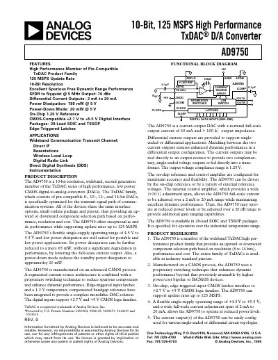
The AD9750 is a high‑performance, 10‑bit, 125 MSPS TxDAC® digital‑to‑analog converter designed for wideband communication and instrumentation. It features differential current outputs (2 mA‑20 mA), an on‑chip 1.20 V bandgap reference, CMOS‑compatible digital interface, and operates from a single supply of 4.5‑5.5 V (AVDD) and 2.7‑5.5 V (DVDD). Power dissipation is low (190 mW typical) and a power‑down mode reduces standby draw to about 20 mW.
The datasheet provides detailed DC, dynamic and digital specifications, pin configuration, absolute maximum ratings, and ordering information for the 28‑lead SOIC and TSSOP packages. Typical application circuits, functional block diagrams and performance graphs illustrate the device’s linearity, spurious‑free dynamic range and settling behavior.
| Resolution | 10 Bits |
|---|---|
| Full‑Scale Output Current | 2 – 20 mA |
| Output Compliance Range | 1.25 V |
| Power Dissipation (5 V, IOUTFS=20 mA) | 190 mW typical |
| Supply Voltage AVDD | 4.5 – 5.5 V |
| Maximum Output Update Rate | 125 MSPS |
The AD9750 can operate at up to 125 MSPS update rate.
The full‑scale current is set by an external resistor RSET that defines the reference current, which is then multiplied by 32.
Typical power dissipation is 190 mW when powered at 5 V with a 20 mA full‑scale output.
Yes, connecting REFLO to AVDD disables the internal reference so an external reference can be used.