
AD5570 is a 16-bit serial input voltage output DAC with a working voltage range of ±12 V/±15 V. It has 1 LSB maximum INL and DNL, and an output voltage range of up to ±14 V. It has a settling time of 10 μs and is suitable for applications such as industrial automation, automatic test equipment, process control, data acquisition systems, and general-purpose instrumentation.
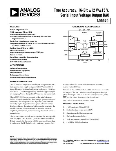
The AD5570 is a single 16‑bit serial‑input, voltage‑output DAC that operates from ±11.4 V to ±16.5 V supplies. It provides full 16‑bit performance with 1 LSB maximum INL and DNL, on‑board reference buffers, and a versatile 3‑wire interface compatible with SPI, QSPI, MICROWIRE and DSP standards.
The device includes features such as a clear (CLR) pin to reset the output to 0 V, a power‑down (PD) pin for low‑power mode, and a high‑voltage‑tolerant ESD rating of 5 kV HBM. It is supplied in a 16‑lead SSOP package and is supported by an evaluation board and extensive microprocessor interfacing examples.
| Resolution | 16 Bits |
|---|---|
| Supply Voltage Range | ±11.4 V to ±16.5 V |
| Output Voltage Range | ±14 V |
| Power‑Down Current | 16 µA |
| Settling Time | 12‑16 µs (16‑bit, ±0.5 LSB) |
| Bandwidth | 20 kHz |
| ESD Rating | 5 kV HBM |
| Operating Temperature Range | −40 °C to +125 °C (W/Y grades) |
The AD5570 operates from ±11.4 V to ±16.5 V supplies.
By asserting the active‑low CLR pin, which resets VOUT to AGND.
The maximum SCLK frequency in standalone mode is 10 MHz.
The device is rated for 5 kV HBM ESD protection.