
This document describes the features and characteristics of the AD5330/AD5331/AD5340/AD5341 series products, including operating voltage range, power consumption, interface type, output range, etc.
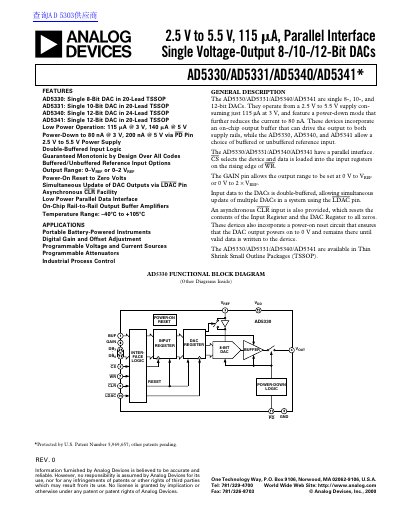
The AD5330, AD5331, AD5340, and AD5341 are single‑channel 8‑, 10‑ and 12‑bit digital‑to‑analog converters that operate from a 2.5 V to 5.5 V supply and feature low power consumption, rail‑to‑rail output, and selectable buffered or unbuffered reference inputs. They include a parallel interface with double‑buffered input logic, power‑down mode, and simultaneous update capability via the LDAC pin.
These devices are intended for portable battery‑powered instruments, programmable voltage/current sources, digital gain and offset adjustment, and industrial process control. The handbook details electrical specifications, timing diagrams, pin descriptions, absolute‑maximum ratings, and example circuits for bipolar operation and multi‑device decoding.
| Resolution (AD5330) | 8 bits |
|---|---|
| Resolution (AD5331) | 10 bits |
| Resolution (AD5340/AD5341) | 12 bits |
| Supply Voltage Range | 2.5 V to 5.5 V |
| Power‑Down Current (3 V) | 80 nA |
| Typical Power Consumption (3 V) | 115 µA |
| Output Voltage Range | 0 V to VREF or 0 V to 2 VREF |
The devices operate from a supply voltage of 2.5 V to 5.5 V.
All DACs can be updated simultaneously by using a common LDAC pin.
The power‑down current is 80 nA when VDD is 3 V.