
This document describes the features and characteristics of the 16-bit, 4-channel/8-channel, 250 kSPS PulSAR ADC. It features 16-bit resolution with no missing codes, a 4-channel (AD7682)/8-channel (AD7689) multiplexer with choice of inputs, unipolar single-ended, differential (GND sense), and pseudobipolar input modes, a throughput of 250 kSPS, INL of ±0.4 LSB typical, ±1.5 LSB maximum (±23 ppm or FSR), a dynamic range of 93.8 dB, SINAD of 92.5 dB at 20 kHz, THD of -100 dB at 20 kHz, an analog input range of 0 V to VREF with VREF up to VDD, support for multiple reference types including internal selectable 2.5 V or 4.096 V, external buffered (up to 4.096 V), and external (up to VDD), an internal temperature sensor (TEMP), a channel sequencer, selectable 1-pole filter, and busy indicator. It has no pipeline delay, uses a SAR architecture, and operates on a single supply of 2.3 V to 5.5 V with a 1.8 V to 5.5 V logic interface. The serial interface is compatible with SPI, MICROWIRE, QSPI, and other protocols.
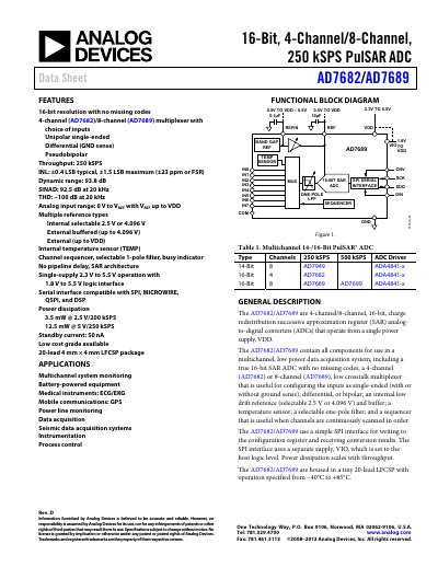
The AD7682 (4‑channel) and AD7689 (8‑channel) are 16‑bit successive‑approximation register (SAR) analog‑to‑digital converters that operate from a single 2.3 V‑5.5 V supply. They include an internal selectable reference, temperature sensor, one‑pole filter, and optional busy indicator, making them suitable for multichannel, low‑power data‑acquisition systems.
Key features include unipolar, differential and pseudobipolar input configurations, a 250 kSPS maximum conversion rate, low power dissipation (as low as 3.5 mW at 200 kSPS) and operation over –40 °C to +85 °C. The datasheet details pin configurations, timing specifications, absolute maximum ratings, and recommended layout guidelines.
| Resolution | 16 bits |
|---|---|
| Throughput | 250 kSPS |
| Supply Voltage | 2.3 V to 5.5 V |
| Input Voltage Range (unipolar) | 0 V to VREF |
| Integral Linearity (INL) | ±0.4 LSB typical |
| Operating Temperature Range | -40 °C to +85 °C |
The devices can sample up to 250 kSPS.
The AD7682 operates from 2.3 V to 5.5 V.
Yes, an optional busy indicator is available for host interfacing.
The ADC supports unipolar single‑ended, differential, and pseudobipolar inputs.