
µPB1508GV is a 3.0 GHz input divide by 2 prescaler IC for DBS tuner applications. µPB1508GV can make VHF/UHF band PLL frequency synthesizer apply to DBS/ECS tuners. µPB1508GV is a shrink package version of µPB584G so that this small package contributes to reduce the mounting space. µPB1508GV is manufactured using NEC’s high fT NESAT™ IV silicon bipolar process. This process uses silicon nitride passivation film and gold electrodes. These materials can protect chip surface from external pollution and prevent corrosion/migration. Thus, this IC has excellent performance, uniformity and reliability.
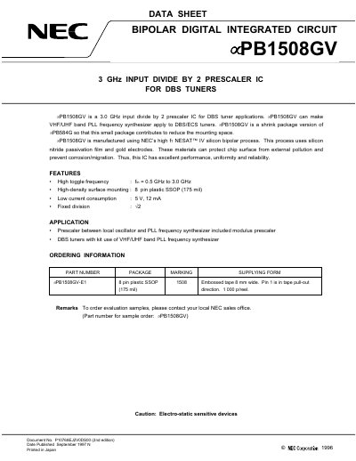
The uPB1508GV is a bipolar digital integrated circuit that divides a 0.5 GHz to 3.0 GHz input frequency by 2 for DBS tuner applications. The document lists its features, typical applications, ordering information, pin assignments, and internal block diagram.
Electrical characteristics such as supply voltage, current consumption, output power, and absolute maximum ratings are detailed, along with recommended operating conditions, test circuits, and soldering guidelines. Handling precautions for electro‑static sensitive devices are also included.
| Input frequency range | 0.5 GHz to 3.0 GHz |
|---|---|
| Supply voltage (Vcc) | 4.5 V to 5.5 V |
| Maximum supply voltage | 6.0 V |
| Circuit current (typical) | 12 mA |
| Package | 8‑pin plastic SSOP (175 mil) |
| Operating temperature range | -40 °C to +85 °C |
The recommended supply voltage is 4.5 V to 5.5 V.
Connect a 1 000 pF bypass capacitor to the Vcc pin to minimize ground impedance.
Infrared ray reflow with a package peak temperature of 235 °C for up to 30 s is recommended.