
HCC4011B,HCF4011B are dual-input, HCC4012B is four-input, and HCF4012B is three-input HCC/HCF4011B, HCF4012B and HCF4023B NAND gate circuits, whose inputs and outputs are all buffered.
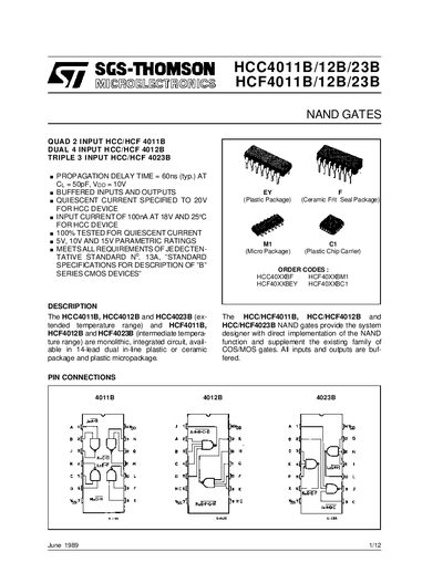
This handbook describes the HCC4011B, HCC4012B, HCC4023B (extended temperature range) and the HCF4011B, HCF4012B, HCF4023B (intermediate temperature range) NAND gate devices. It lists package options (14‑lead DIP, ceramic, micropackage, PLCC20) and shows pin connections for each package type.
Key electrical data include propagation delay, quiescent input current, supply voltage limits, power dissipation, and temperature ranges. Static and dynamic characteristics are given for typical operating conditions, along with typical output source/sink currents, voltage transfer curves, and mechanical dimensions for the DIP14 and PLCC20 packages.
| Propagation Delay Time (typ.) | 60 ns |
|---|---|
| Quiescent Input Current | 100 nA |
| Supply Voltage Range (HCC) | 0.5 V to 20 V |
| Total Power Dissipation (per package) | 200 mW |
| Operating Temperature Range (HCC) | -55 °C to +125 °C |
| Input Capacitance (any input) | 5 pF to 7.5 pF |
The typical propagation delay time is 60 ns.
The quiescent input current is 100 nA.