
MAX7306/MAX7307 is an I2C-compatible, serial-interfaced four-level translating I/O device operating from 1.62V to 3.6V. The MAX7307 features a port supply (VLA) that allows level translation on I/O ports to operate from a separate power supply from 1.4V to 5.5V. The MAX7306 features an address select input (AD0) to allow up to four unique slave addresses. MAX7306/MAX7307 ports P2, P3 and P4 can be configured as inputs, push-pull outputs and open-drain outputs. Port P1 can be configured as a general-purpose input, open-drain output or an open-drain INT output. Ports P2 and P3 can be configured as OSCIN and OSCOUT respectively. The MAX7306/MAX7307 include an internal oscillator for PWM, blink and key debounce or to cascade multiple MAX7306/MAX7307s. The external clock can be used to set a specific PWM and blink timing. The RST input asynchronously clears the 2-wire interface and terminates a bus lockup involving the MAX7306/MAX7307. All ports configured as output feature 33-step PWM, allowing any output to be set from fully off, 1/32 to 31/32 duty cycle, to fully on. All output ports also feature LED blink control, allowing blink periods of 1/8 second, 1/4 second, 1/2 second, 1, 2, 4 or 8 seconds. Any port can blink during this period with a 1/16 to 15/16 duty cycle. MAX7306/MAX7307 are specified over the -40°C to +125°C temperature range and are available in 10-pin µDFN (2mm x 2mm) and 10-pin µMAX®.
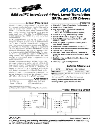
The MAX7306 and MAX7307 are SMBus/I²C‑compatible 4‑port GPIO expanders with level‑translating I/O. They operate from a 1.62 V to 3.6 V supply (MAX7306) or 1.40 V to 5.5 V port‑supply (MAX7307) and include an internal oscillator for PWM, blink, and key‑debounce functions. Each port can be configured as input, push‑pull output, or open‑drain output, and the devices support up to 25 mA sink per port with a total of 100 mA across all ports.
The datasheet details absolute maximum ratings, electrical characteristics, timing specifications, pin descriptions, register maps, and ordering information. It also lists typical applications such as LCD/keypad backlights, LED status indicators, and cell‑phone I/O expansion, and provides package options (10‑pin UDFN and UMAX).
| Operating Supply Voltage | 1.62 V to 3.60 V |
|---|---|
| Port Logic Supply Voltage (VLA) | 1.40 V to 5.50 V |
| Standby Current (typ) | 0.75 µA |
| Maximum Sink Current per Port | 25 mA (100 mA total) |
| Output Low Voltage (P1‑P4) | 0.19 V to 0.40 V (typ 0.25 V) |
| Output High Voltage (P2‑P4) | 2.5 V ± 0.3 V (typ) |
| Package Types | 10‑pin UDFN (2 mm × 2 mm) and 10‑pin UMAX |
The devices operate from 1.62 V to 3.60 V supply voltage.
Each output port can sink up to 25 mA, with a total sink capability of 100 mA across all ports.
They are offered in 10‑pin UDFN (2 mm × 2 mm) and 10‑pin UMAX packages.
Typical standby current is 0.75 µA.