
This document describes the features and characteristics of the FDS8880 N-Channel PowerTrench® MOSFET product released in April 2007, including low rDS(on), low gate charge, high power and current handling capability, etc.
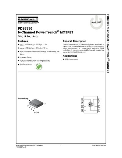
The FDS8880 is a N‑Channel PowerTrench MOSFET designed for high‑efficiency DC/DC converters. It offers low on‑resistance, low gate charge and high current handling capability, making it suitable for both synchronous and conventional switching applications.
The datasheet provides maximum ratings, detailed electrical and switching characteristics, thermal performance data, and SPICE models for circuit designers. It also includes guidelines for thermal management and mounting pad considerations.
| Drain to Source Voltage (VDSS) | 30 V |
|---|---|
| Gate to Source Voltage (VGS) | ±20 V |
| Continuous Drain Current (ID) | 11.6 A |
| On‑Resistance (rDS(on)) at VGS=10V | 10 mΩ |
| Maximum Power Dissipation (PD) | 2.5 W |
The device can handle a continuous drain current of 11.6 A at VGS = 10 V.
The typical on‑resistance is 10 mΩ when VGS is 10 V.
The MOSFET is rated for a maximum drain‑to‑source voltage of 30 V.