
The CD4001BC/CD4011BC is a quad 2-input NOR buffered B series gate/quad 2-input NAND buffered B series gate
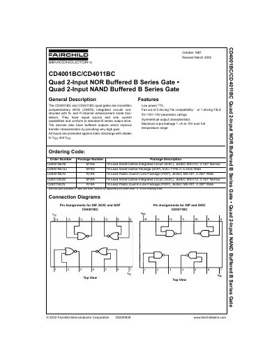
The CD4001BC and CD4011BC are monolithic complementary MOS (CMOS) quad gates with buffered outputs that deliver very high gain and improve transfer characteristics. All inputs are protected against static discharge with diodes to VDD and VSS, and the devices conform to the standard B‑series output drive.
The document lists detailed electrical parameters such as supply voltage range, power dissipation, propagation delays, and input leakage. It also includes pin‑assignment tables for DIP, SOIC, and SOP packages, as well as physical dimensions and ordering codes for each package type. This manual is written in Chinese.
| Supply voltage range | −0.5 VDC to +18 VDC |
|---|---|
| Power dissipation (PD) | 700 mW (PDIP) / 500 mW (SOIC) |
| Operating temperature range | −55 °C to +125 °C |
| Maximum input leakage current | 1 µA at 15 V |
The devices can operate with a supply voltage up to +18 VDC.