
The LM2662/LM2663 CMOS charge-pump voltage converter inverts a positive voltage in the range of 1.5V to 5.5V to the corresponding negative voltage. The LM2662/LM2663 uses two low cost capacitors to provide 200 mA of output current without the cost, size, and EMI related to inductor based converters. With an operating current of only 300 µA and operating efficiency greater than 90% at most loads, the LM2662/LM2663 provides ideal performance for battery powered systems. The LM2662/LM2663 may also be used as a positive voltage doubler. The oscillator frequency can be lowered by adding an external capacitor to the OSC pin. Also, the OSC pin may be used to drive the LM2662/LM2663 with an external clock. For LM2662, a frequency control (FC) pin selects the oscillator frequency of 20 kHz or 150 kHz. For LM2663, an external shutdown (SD) pin replaces the FC pin. The SD pin can be used to disable the device and reduce the quiescent current to 10 µA. The oscillator frequency for LM2663 is 150 kHz.
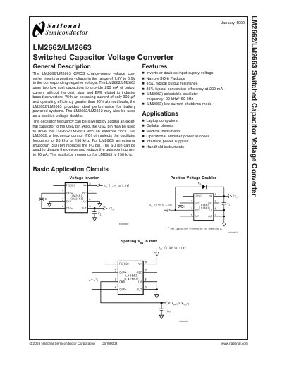
The LM2662 and LM2663 are CMOS charge‑pump converters that invert a positive input voltage of 1.5 V to 5.5 V, delivering up to 200 mA of negative output current. They use two low‑cost external capacitors, achieve over 90 % efficiency at typical loads, and can also operate as a positive voltage doubler.
The document provides absolute maximum ratings, detailed electrical characteristics, typical performance graphs, connection diagrams for the 8‑lead SO package, and a range of application examples such as simple negative‑voltage converters, voltage doublers, and cascaded or parallel configurations. It also includes physical dimensions, life‑support policy, and compliance information.
| Input voltage range | 1.5 V to 5.5 V |
|---|---|
| Maximum output current | 200 mA |
| Quiescent current (LM2662) | 300 µA |
| Shutdown current (LM2663) | 10 µA |
| Oscillator frequency (LM2662) | 20 kHz or 150 kHz |
| Oscillator frequency (LM2663) | 150 kHz |
| Package | Narrow SO‑8 |
| Typical output resistance | 3.5 Ω |
| Typical conversion efficiency (200 mA) | 86 % |
It operates with an input voltage from 1.5 V up to 5.5 V.
The converter can deliver up to 200 mA of output current.
The FC pin selects the frequency: open gives 20 kHz, tying it to V+ gives 150 kHz.
By applying a voltage to the SD pin to enter shutdown mode, lowering the current to 10 µA.