
The MAX4539/MAX4540 low-voltage, CMOS 8-channel (MAX4539) and dual 4-channel (MAX4540) multiplexers are ideal for precision ADC calibration and system self-monitoring applications. These calibration multiplexers (cal-muxes) have precision resistor-dividers to generate accurate voltage ratios from an input reference voltage. The reference ratios include 15/4096 and 4081/4096 of the external reference voltage, accurate to 15 bits, and 1/2V+ and 5/8(V+ - V-), accurate to 8 bits. The external reference voltage as well as ground can also be switched to the output. The MAX4539/MAX4540 have enable inputs and address latching. All digital inputs have 0.8V and 2.4V logic thresholds, ensuring both TTL- and CMOS-logic compatibility when using a ±5V or a single +5V supply. Protection diodes at all inputs provide an ESD rating >2kV. The MAX4539/MAX4540 operate from a single +2.7V to +12V supply, or from dual supplies of ±2.7V to ±6V. On-resistance (100Ω max) is matched between switches to 6Ω max. Each switch can handle Rail-to-Rail® analog signals. The off leakage current is 0.1nA at TA = +25°C and 2nA at TA = +85°C. The MAX4539/MAX4540 are available in small 20-pin DIP, SO, and SSOP packages.
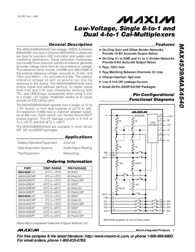
The MAX4539 (single 8‑to‑1) and MAX4540 (dual 4‑to‑1) are low‑voltage CMOS calibration multiplexers that provide accurate voltage ratios for precision ADC calibration and system self‑monitoring. They include on‑chip gain and offset divider networks that generate 15‑bit and 8‑bit accurate output ratios, and feature enable inputs and address latching.
The devices operate from a single +2.7 V to +12 V supply (or dual +2.7 V to +6 V), have on‑resistance up to 100 Ω with channel matching within 6 Ω, and exhibit an off‑leakage current of 0.1 nA. They are offered in 20‑pin SSOP, wide‑SO, and plastic DIP packages and support TTL‑ and CMOS‑compatible logic levels (0.8 V – 2.4 V).
| Supply voltage range (single supply) | +2.7 V to +12 V |
|---|---|
| Supply voltage range (dual supplies) | +2.7 V to +6 V |
| On‑Resistance (Ron) max | 100 Ω |
| Ron matching between channels | 6 Ω max |
| Off‑leakage current | 0.1 nA (typical at 25 °C) |
| Logic input thresholds | 0.8 V (low) – 2.4 V (high) |
| Package types | 20‑pin SSOP, wide‑SO, plastic DIP |
| Enable inputs and address latch | Provided |
They operate from a single +2.7 V to +12 V supply, or from dual supplies of +2.7 V to +6 V.
The on‑resistance is specified as 100 Ω max, with channel matching within 6 Ω.
The off‑leakage current is 0.1 nA at 25 °C (and similar at higher temperatures).
They are offered in 20‑pin SSOP, wide‑SO, and plastic DIP packages.