
The MAX4721/MAX4722/MAX4723 are low-voltage, low on-resistance dual single-pole/single throw (SPST) analog switches that operate from a single +1.8V to +5.5V supply. These devices are designed for USB 1.1 and audio switching applications. The MAX4721/MAX4722/MAX4723 feature 4.5Ω on-resistance (max) with 1.2Ω flatness and 0.3Ω matching between channels. These new switches operate from +1.8V to +5.5V and are fully specified at 3V and 5V. They offer break-before-make switching (1ns) with tON <80ns and tOFF <40ns at +2.7V. The digital logic inputs are +1.8V logic compatible with a +2.7V to +3.6V supply. These switches are packaged in a chip-scale package (UCSP™), significantly reducing the required PC board area. The chip occupies only a 1.52mm ✕ 1.52mm area and has a 3 ✕ 3 bump array with a bump pitch of 0.5mm. They are also available in an 8-pin µMAX package.
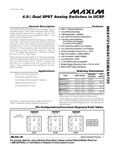
The MAX4721, MAX4722, and MAX4723 are low‑voltage, low‑on‑resistance dual single‑pole/single‑throw (SPST) analog switches that operate from a single +1.8 V to +5.5 V supply. They are designed for USB 1.1 and audio‑switching applications and are offered in a chip‑scale UCSP package as well as an 8‑pin µMAX package.
Key features include 4.5 Ω (max) on‑resistance, break‑before‑make switching, low leakage (<0.5 nA), high off‑isolation (‑55 dB), low crosstalk (‑80 dB), >300 MHz bandwidth, and CMOS‑logic compatible inputs. Detailed electrical characteristics, pin configurations, and test circuits are provided for designers.
| On‑Resistance (R_ON) max at 3 V | 4.5 Ω |
|---|---|
| On‑Resistance Match Between Channels | 0.3 Ω max |
| Turn‑Off Time (t_OFF) | <40 ns at +2.7 V |
| Leakage Current | <0.5 nA at 25 °C |
| Off‑Isolation | -55 dB (10 MHz) |
| Crosstalk | -80 dB (10 MHz) |
| Bandwidth (3‑dB) | >300 MHz |
| Total Harmonic Distortion | 0.03 % |
The on‑resistance is 4.5 Ω max at a 3 V supply.
Leakage current is less than 0.5 nA at 25 °C.