
The MAX5181/MAX5184 are 10-bit, current-output digital-to-analog converters (DACs) designed for superior performance in signal reconstruction or arbitrary waveform generation applications requiring analog signal reconstruction with low distortion and low-power operation. The MAX5184 provides equal specifications, with on-chip precision resistors for voltage-output operation. The MAX5181/MAX5184 are designed for a 10pVs glitch operation to minimize unwanted spurious signal components at the output. An on-board 1.2V bandgap circuit provides a well-regulated, low-noise reference that can be disabled for external reference operation. The devices are designed to provide a high level of signal integrity for the least amount of power dissipation. They operate from a single 2.7V to 3.3V supply. Additionally, these DACs have three modes of operation: normal, low-power standby, and full shutdown, which provides the lowest possible power dissipation with a 1µA (max) shutdown current. A fast wake-up time (0.5µs) from standby mode to full DAC operation facilitates power conservation by activating the DAC only when required. The MAX5181/MAX5184 are available in 24-pin QSOP packages and are specified for the extended (-40°C to +85°C) temperature range. Additionally, the MAX5184 is also available in a 24-pin TQFN with exposed pad (EP) and is specified for the extended (-40°C to +85°C) temperature range. For lower resolution, 8-bit versions, refer to the MAX5187/MAX5188.
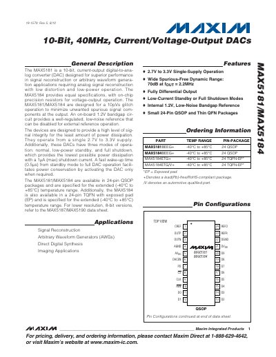
The Maxim MAX5181 and MAX5184 are 10‑bit digital‑to‑analog converters designed for signal reconstruction and arbitrary waveform generation. They operate from a single 2.7 V to 3.3 V supply and are available in 24‑pin QSOP and TQFN packages rated for –40 °C to +85 °C.
The devices feature three power‑down modes (normal, low‑power standby, full shutdown), an internal 1.2 V low‑noise bandgap reference, and up to 1.5 mA full‑scale output current. Detailed electrical characteristics, timing diagrams, pin descriptions and layout recommendations are provided.
| Supply Voltage | 2.7 V to 3.3 V |
|---|---|
| Resolution | 10 bits |
| Full‑Scale Output Current | 1.5 mA |
| Shutdown Current (max) | 1 µA |
| Standby Current | 1.0 mA to 1.5 mA |
| Operating Temperature Range | -40 °C to +85 °C |
| Clock Frequency | up to 40 MHz |
| Differential Output Resistance | 400 Ω |
The devices operate from a single 2.7 V to 3.3 V supply.
Three modes are provided: normal operation, low‑power standby, and full shutdown.
The shutdown current is limited to a maximum of 1 µA.
The MAX5184 provides a full‑scale output voltage of 400 mV.