
The MAX5180 contains two 10-bit, simultaneous-update, current-output digital-to-analog converters (DACs) designed for superior performance in communications systems requiring analog signal reconstruction with low distortion and low-power operation. The MAX5183 provides equal specifications, with on-chip precision resistors for voltage output operation. The devices are designed for 10pVs glitch operation to minimize unwanted spurious signal components at the output.
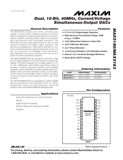
The MAX5180 and MAX5183 are dual, 10‑bit digital‑to‑analog converters designed for high‑speed signal reconstruction in communication systems. They operate from a single 2.7 V to 3.3 V supply, provide simultaneous current (MAX5180) or voltage (MAX5183) outputs, and include an on‑chip 1.2 V low‑noise bandgap reference.
Three power‑down modes (normal, low‑power standby, and shutdown) enable ultra‑low power consumption, with a maximum shutdown current of 1 µA. The devices are supplied in a 28‑pin QSOP package and are specified for an extended temperature range of –40 °C to +85 °C. Detailed electrical characteristics, pin descriptions, timing diagrams, and application notes are provided.
| Supply Voltage (AVDD/DVDD) | 2.7 V to 3.3 V |
|---|---|
| Resolution | 10‑bit |
| Maximum Clock Frequency | 40 MHz |
| Full‑Scale Output Current (MAX5180) | 1 mA into 400 Ω load |
| Full‑Scale Output Voltage (MAX5183) | 400 mV differential |
| Shutdown Current (max) | 1 µA |
| Operating Temperature Range | –40 °C to +85 °C |
| Package | 28‑pin QSOP |
| Bandgap Reference Voltage | 1.2 V |
| Spurious‑Free Dynamic Range | 70 dB at fOUT = 2.2 MHz |
The devices operate from a single supply voltage of 2.7 V to 3.3 V.
Three modes are available: normal operation, low‑power standby, and complete shutdown.
The maximum shutdown current is 1 µA.
Both devices are supplied in a 28‑pin QSOP package.