
The ADN2891 is a 3.2Gbps limiting amplifier with integrated loss-of-signal (LOS) detection circuitry and a received signal strength indicator (RSSI). This part is optimized for SONET, Gigabit Ethernet (GbE), and Fibre Channel optoelectronic conversion applications. The ADN2891 has a differential input sensitivity of 4 mV p-p and accepts up to a 2.0 V p-p differential input overload voltage. The ADN2891 supports current mode logic (CML) outputs with controlled rise and fall times. 80 ps rise/fall times CML outputs: 700 mV p-p differential Programmable LOS detector: 3.5 mV to 35 mV Rx signal strength indicator (RSSI) SFF-8472-compliant average power measurement Single-supply operation: 3.3 V Low power dissipation: 145 mW Available in
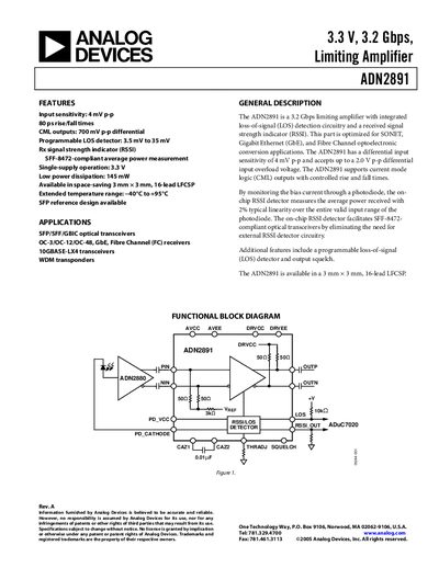
The ADN2891 is a 3.2 Gbps limiting amplifier featuring integrated loss‑of‑signal detection and a received‑signal‑strength indicator (RSSI). It is optimized for SONET, Gigabit Ethernet, and Fibre Channel applications and operates from a single 3.3 V supply with low power dissipation (145 mW). The device is available in a compact 3 mm × 3 mm, 16‑lead LFCSP package and supports an extended temperature range of –40 °C to +95 °C.
Key specifications include a differential input sensitivity of 4 mV p‑p, 80 ps rise/fall times, and CML output swing of 600‑850 mV p‑p. The part also provides programmable LOS thresholds, output squelch, and a photodiode‑biased RSSI circuit that complies with SFF‑8472 optical‑transceiver standards.
| Input Voltage Range | 1.8 V to 2.8 V p‑p |
|---|---|
| Input Sensitivity | 4 mV p‑p |
| Rise/Fall Time | 80 ps |
| Output Voltage Swing | 600 mV to 850 mV p‑p differential |
| Operating Temperature Range | –40 °C to +95 °C |
| Power Dissipation | 145 mW |
| Package | 3 mm × 3 mm, 16‑lead LFCSP |
The ADN2891 accepts an input voltage range of 1.8 V to 2.8 V p‑p.
It operates from –40 °C up to +95 °C.
The differential output swing is specified as 600 mV to 850 mV p‑p.