
This document is a reference design manual for 3.3V 2.7 Gb/s Limiting Amplifier ADN2890, introducing the main features and characteristics of the product.
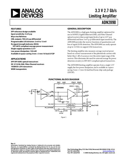
The ADN2890 limiting amplifier is designed for SONET, Gigabit Ethernet, and Fibre Channel optical receivers. It accepts up to 2.0 V p‑p differential input and provides 3 mV p‑p input sensitivity, with built‑in loss‑of‑signal detection and a received‑signal‑strength indicator.
Key features include single‑supply 3.3 V operation, 130 mW power dissipation, 700 mV p‑p differential output swing, 80 ps rise/fall time, and operation over –40 °C to +85 °C. The device is offered in a 3 mm × 3 mm 16‑lead LFCSP package.
| Input Sensitivity | 3 mV p‑p |
|---|---|
| Supply Voltage | 3.3 V (single‑supply) |
| Power Dissipation | 130 mW |
| Output Voltage Swing | 700 mV p‑p differential (typical) |
| Output Rise/Fall Time | 80 ps (typical) |
| Operating Temperature Range | –40 °C to +85 °C |
| Package | 16‑lead 3 mm × 3 mm LFCSP |
The ADN2890 has an input sensitivity of 3 mV p‑p.
It operates from a single 3.3 V supply.
Yes, the device integrates a LOS detector with an adjustable threshold.
It has an on‑chip RSSI circuit that converts photodiode current to a proportional voltage.