
CY74FCT163501 and CY74FCT163H501 are 18-bit registered transceivers with low power consumption, 5V compatible inputs and outputs, 24mA balanced drive outputs, power-off disable outputs, edge rate control circuitry, FCT-C speed of 4.6ns, latch-up performance exceeding JEDEC standard 17, ESD>2000V, typical output skew<250ps, industrial temperature range of -40°C to +85°C, TSSOP (19.6-mil pitch) or SSOP (25-mil pitch), typical VOLP (ground bounce) performance exceeding Mil Std 883D, VCC=2.7V to 3.6V.
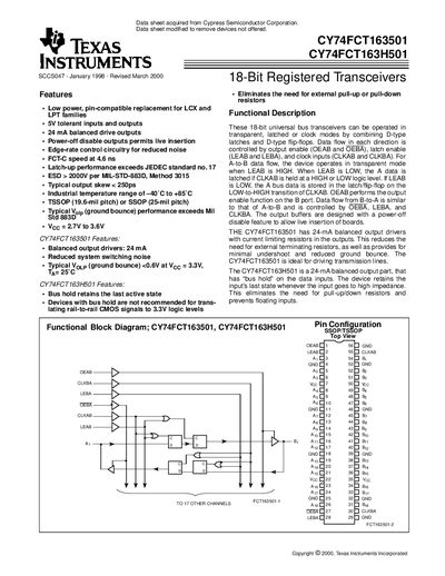
The CY74FCT163501 and CY74FCT163H501 are 18‑bit universal bus transceivers offering low‑power, balanced 24 mA output drivers and optional bus‑hold functionality. They support transparent, latched and clocked operation with separate A‑to‑B and B‑to‑A control signals, making them suitable for driving transmission lines and eliminating the need for external pull‑up/down resistors.
The devices are available in TSSOP (19.6‑mil pitch) and SSOP (25‑mil pitch) packages, operate over an industrial temperature range of –40 °C to +85 °C, and meet JEDEC latch‑up and MIL‑STD‑883E ESD specifications. Detailed electrical characteristics, switching parameters, and ordering information are provided in the following sections.
| Balanced output driver current | 24 mA |
|---|---|
| Input high voltage range | 2.0 V to 5.5 V |
| Propagation delay (typical) | 4.6 ns |
| Operating temperature range | –40 °C to +85 °C |
| Package types | TSSOP, SSOP |
| ESD rating | >2000 V (MIL‑STD‑883D, Method 3015) |
The maximum input high voltage is 5.5 V.
Yes, the CY74FCT163H501 includes bus‑hold on the data inputs, retaining the last state when inputs go high‑impedance.
Typical propagation delay is 4.6 ns.
They are offered in 56‑lead TSSOP and SSOP packages.