
LMH0346 3 Gbps HD/SD SDI Reclocker is a chip that can re-time digital video data. It conforms to the SMPTE 424M, SMPTE 292M, and SMPTE 259M (C) standards. The chip operates at data rates of 270 Mbps, 1.483 Gbps, 1.485 Gbps, 2.967 Gbps, and 2.97 Gbps. LMH0346 supports DVB-ASI operation at 270 Mbps. LMH0346 automatically detects the incoming data rate and adjusts itself to retime the incoming data to suppress accumulated jitter. LMH0346 also recovers the serial data-rate clock and optionally provides it as an output. LMH0346 has two differential serial data outputs, the second output can be selected as a low-jitter, data-rate clock output. Controls and indicators are: serial clock or second serial data output select, manual rate select input, SD/HD rate indicator output, lock detect output, auto/manual data bypass and output mute. The serial data inputs, outputs, and serial clock outputs are differential LVPECL compatible. The CML serial data and serial clock outputs are suitable for driving 100 Ω differentially terminated networks. The control logic inputs and outputs are LVCMOS compatible. LMH0346 is powered from a single 3.3V supply. Typical power dissipation is 370 mW. The device is available in two space–saving packages: a 6.5 X 4.4 mm 20-pin e-TSSOP and an even more space–efficient 5 X 4 mm 24-pin LLP package.
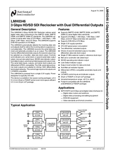
The LMH0346 3 Gbps HD/SD SDI Reclocker retimes serial video data and automatically detects the incoming data rate, providing two low‑jitter differential outputs. It supports SMPTE 259M (C), SMPTE 292M, SMPTE 424M, and DVB‑ASI at 270 Mbps, making it suitable for digital video routers, switchers, processing and editing equipment, and format converters.
The device is supplied in a 20‑pin e‑TSSOP or a 24‑pin LLP package, both with an exposed die‑attach pad tied to ground. It operates from a single 3.3 V supply with typical power consumption of 370 mW. Pin functions include data‑rate selection, lock‑detect, output‑mute, and a 27 MHz reference clock input, allowing flexible configuration of the second output as either data or a clock signal.
| Supply voltage | Single 3.3 V |
|---|---|
| Typical power consumption | 370 mW |
| Differential output level | 750 mV p‑p |
| Reference clock input | 27 MHz external crystal or oscillator |
| Lock‑detect output | Active‑high PLL lock detect |
| Output mute function | Mutes data and clock outputs when low |
The device operates from a single 3.3 V supply and typically consumes 370 mW of power.
The SCO_EN pin selects the mode; when high, the SCO/SDO2 output provides a serial clock, otherwise it provides retimed serial data.