
The ADC08100 is a low-power, 8-bit, monolithic analog-to- digital converter with an on-chip track-and-hold circuit. Optimized for low cost, low power, small size and ease of use, this product operates at conversion rates of 20 MSPS to 100 MSPS with outstanding dynamic performance over its full operating range while consuming just 1.3 mW per MHz of clock frequency. That’s just 130 mW of power at 100 MSPS. Raising the PD pin puts the ADC08100 into a Power Down mode where it consumes just 1 mW. The unique architecture achieves 7.4 Effective Bits with 41 MHz input frequency. The excellent DC and AC charac- teristics of this device, together with its low power consump- tion and single +3V supply operation, make it ideally suited for many imaging and communications applications, includ- ing use in portable equipment. Furthermore, the ADC08100 is resistant to latch-up and the outputs are short-circuit proof. The top and bottom of the ADC08100’s reference ladder are available for connections, enabling a wide range of input possibilities. The digital outputs are TTL/CMOS compatible with a separate output power supply pin to support interfac- ing with 3V or 2.5V logic. The digital inputs (CLK and PD) are TTL/CMOS compatible. The ADC08100 is offered in a 24-lead plastic package (TSSOP) and is specified over the industrial temperature range of −40˚C to +85˚C. An evaluation board is available to assist in evaluating device performance.
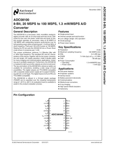
The ADC08100 is a low‑power, 8‑bit monolithic analog‑to‑digital converter with an on‑chip track‑and‑hold circuit. It operates at conversion rates of 20 MSPS to 100 MSPS while consuming only 1.3 mW per MHz of clock frequency, making it suitable for portable imaging and communications equipment.
Key features include single‑ended input, internal sample‑and‑hold, low‑voltage single‑+3 V operation, a 24‑lead TSSOP package, and a power‑down mode. The device offers TTL/CMOS‑compatible digital I/O, a reference ladder with external connections, and an evaluation board for quick testing.
| Resolution | 8 bits |
|---|---|
| Effective Number of Bits (ENOB) | 7.4 bits (typ) |
| Differential Non‑Linearity (DNL) | 0.4 LSB (typ) |
| Total Harmonic Distortion (THD) | -60 dB (typ) |
| Power Consumption | 1.3 mW per MHz (typ) |
| Maximum Sampling Frequency | 100 MSPS (min) |
| Supply Voltage (Vv) | 3.8 V |
| Operating Temperature Range | -40 °C to +85 °C |
| Full Power Bandwidth | 200 MHz |
The device consumes 1.3 mW for each MHz of clock frequency.
All inputs must stay within ±300 mV of the ground or supply pins; exceeding this can cause faulty operation or damage.