
This datasheet introduces the characteristics of ADG5208/ADG5209 high voltage, latch-up proof, 4/8-channel multiplexers. The device is manufactured using a monolithic CMOS process and features low on resistance, low input capacitance, low input current, low shutdown current, low voltage differential configuration and high ESD protection.
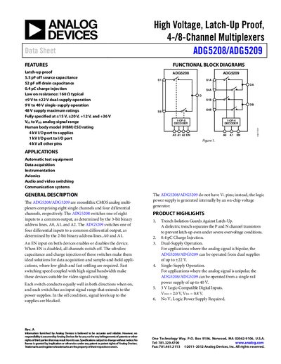
The ADG5208 and ADG5209 are high‑voltage, latch‑up‑proof CMOS analog multiplexers offering 8‑channel (single‑ended) and 4‑channel (differential) configurations. They support dual‑supply operation from +9 V to +22 V or single‑supply operation up to 40 V, making them suitable for data‑acquisition, test equipment, and video‑signal switching applications.
Key features include ultra‑low off‑source capacitance (5.5 pF), low charge injection (0.4 pC), on‑resistance as low as 160 Ω typical, and 3‑V logic‑compatible digital inputs. Detailed specifications, pin configurations, and performance graphs are provided for each supply option.
| On‑Resistance (Ron) typical | 160 Ω |
|---|---|
| Input High Voltage (VIH) | 2.0 V min |
| Input Low Voltage (VIL) | 0.8 V max |
| Charge Injection | 0.4 pC |
| Dual‑Supply Voltage Range | +9 V to +22 V |
| Single‑Supply Voltage Maximum | 40 V |
| Bandwidth (ADG5208) | 54 MHz typ |
The devices can operate with a dual supply from +9 V up to +22 V (and the corresponding negative supply).
The typical on‑resistance is 160 Ω.
The charge injection is 0.4 pC.