
The MAX536/MAX537 combine four 12-bit voltage-output digital-to-analog converters (DACs) and four precision output amplifiers in a space-saving 16-pin package. Offset, gain, and linearity are factory calibrated to provide the MAX536’s ±1LSB total unadjusted error. The MAX537 operates with ±5V supplies, while the MAX536 uses -5V and +12V to +15V supplies. Each DAC has a double-buffered input, organized as an input register followed by a DAC register. A 16-bit serial word is used to load data into each input/DAC register. The serial interface is compatible with either SPI/QSPI™ or Microwire™, and allows the input and DAC registers to be updated independently or simultaneously with a single software command. The DAC registers can be simultaneously updated with a hardware LDAC pin. All logic inputs are TTL/CMOS compatible.
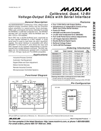
The MAX536 and MAX537 combine four 12‑bit voltage‑output DACs and four precision output amplifiers in a 16‑pin DIP or SO package. They are factory‑calibrated for low total unadjusted error and support independent or simultaneous control of each channel via a 3‑wire serial interface.
Both devices operate from standard supply ranges (MAX536: –5 V to +15 V, MAX537: +5 V) and provide buffered voltage outputs. Detailed electrical characteristics, timing specifications, and package information are provided for designers.
| Resolution | 12 bits |
|---|---|
| Total Unadjusted Error (MAX536) | +1 LSB |
| Positive Supply Range | 10.8 V – 16.5 V |
| Negative Supply Range | 4.5 V – 5.5 V |
| Package Types | 16‑Pin DIP or SO |
| Serial Interface Compatibility | SPI/QSPI and Microwire |
Both devices are compatible with SPI/QSPI and Microwire serial interfaces.
The DACs provide a 12‑bit resolution.
The MAX537 operates from a +5 V supply.
The MAX536 has a total unadjusted error of +1 LSB.