
The MAX1132/MAX1133 are 200ksps, 16-bit ADCs. These serially interfaced ADCs connect directly to SPI™, QSPI™, and MICROWIRE™ devices without external logic. They combine an input scaling network, internal track/hold, clock, a +4.096V reference, and three general-purpose digital output pins (for external multiplexer or PGA control) in a 20-pin SSOP package. The excellent dynamic performance (SINAD ≥ 85dB), high-speed (200ksps), and low power (7.5mA) of these ADCs, make them ideal for applications such as industrial process control, instrumentation, and medical applications. The MAX1132 accepts input signals of 0 to +12V (unipolar) or ±12V (bipolar), while the MAX1133 accepts input signals of 0 to +4.096V (unipolar) or ±4.096V (bipolar). Operating from a single +4.75V to +5.25V analog supply and a +4.75V to +5.25V digital supply, power-down modes reduce current consumption to 1mA at 10ksps and further reduce supply current to less than 20µA at slower data rates. A serial strobe output (SSTRB) allows direct connection to the TMS320 family of digital signal processors. The MAX1132/MAX1133 user can select either the internal clock, or an external serial-interface clock for the ADC to perform analog-to-digital conversions. The MAX1132/MAX1133 feature internal calibration circuitry to correct linearity and offset errors. On-demand calibration allows the user to optimize performance. Three user-programmable logic outputs are provided for the control of a
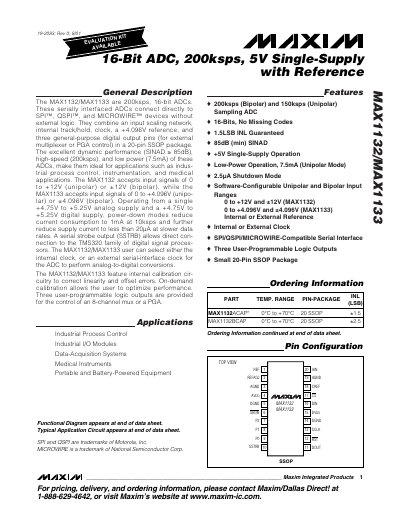
The MAX1132 and MAX1133 are 16‑bit successive‑approximation ADCs that operate from a single 4.75 V–5.25 V supply. They support SPI, QSPI and MICROWIRE interfaces and include an internal reference of +4.096 V, an input scaler, and three user‑programmable logic outputs for external multiplexers or PGA control.
Both devices offer selectable unipolar and bipolar input ranges (MAX1132: 0‑12 V / ±12 V, MAX1133: 0‑4.096 V / ±4.096 V) and provide high dynamic performance with SINAD of at least 85 dB. Power consumption is low, with 7.5 mA typical operation and a 2.5 µA shutdown mode.
| Resolution | 16 bits |
|---|---|
| Sampling Rate (bipolar) | 200 ksps |
| Supply Voltage (analog & digital) | 4.75 V – 5.25 V |
| Typical Power Consumption | 7.5 mA (unipolar mode) |
| Shutdown Current | 2.5 µA |
| Input Range (MAX1132) | 0‑12 V unipolar, ±12 V bipolar |
| Input Range (MAX1133) | 0‑4.096 V unipolar, ±4.096 V bipolar |
| Reference Voltage | +4.096 V |
| SINAD | ≥85 dB |
| User‑Programmable Logic Outputs | 3 (P0, P1, P2) |
Both devices operate from a single 4.75 V to 5.25 V analog and digital supply.
The ADCs provide three push‑pull CMOS outputs (P0, P1, P2).
The maximum bipolar sampling rate is 200 ksps.
The internal reference voltage is +4.096 V.