
This document introduces TC4420/TC4429 6A (peak) single-output MOSFET drivers. These drivers are fabricated in CMOS for lower power and more efficient operation versus bipolar drivers. Both devices have TTL/CMOS compatible inputs that can be driven as high as VDD + 0.3V or as low as –5V without upset or damage to the device. This eliminates the need for external level-shifting circuitry and its associated cost and size. The output swing is rail-to-rail, ensuring better drive voltage margin, especially during power-up/power-down sequencing. Propagational delay time is only 55 ns (typ.) and the output impedance is 2.5 Ω.
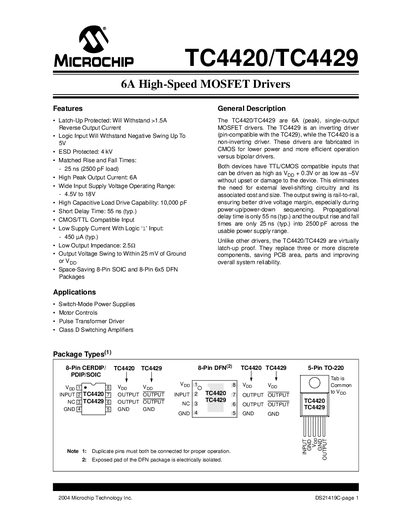
The TC4420/TC4429 family are 6 A peak, single‑output MOSFET drivers. The TC4420 provides a non‑inverting output, while the TC4429 offers an inverting output and is pin‑compatible with the TC4420. Both devices feature latch‑up protection, ESD protection, and CMOS/TTL compatible inputs.
Electrical specifications include a 4.5 V‑18 V supply range, 25 ns rise/fall times into 2500 pF loads, 55 ns typical propagation delay, and a low supply current of 450 pA with a logic‑high input. The drivers are available in 8‑pin SOIC, 8‑pin DFN, and other package options, with detailed pin descriptions and recommended external components provided.
| Peak Output Current | 6 A |
|---|---|
| Input Supply Voltage Range | 4.5 V to 18 V |
| Latch‑Up Protection Current | >1.5 A |
| Rise/Fall Time (2500 pF load) | 25 ns |
| Typical Propagation Delay | 55 ns |
| Supply Current (Logic ‘1’ input) | 450 pA |
The TC4420 is a non‑inverting driver, while the TC4429 is an inverting driver and they are pin‑compatible.
The typical propagation delay is 55 ns.
The drivers operate from 4.5 V to 18 V.