
The LP3950 is a color LED driver with a built-in audio synchronization feature for any analog audio input such as polyphonic ring tones and MP3 music. LEDs can be synchronized to an audio signal with two methods - amplitude and frequency. Also several fine tuning options are available for differentiation purposes. The chip also has an unique AGC (Automatic Gain Control) feature which tracks the input signal level and automatically adjusts the gain to an optimal value. The LP3950 has a high efficiency magnetic DC/DC converter with programmable output voltage and switching frequency. The converter has high output current capability so it is also able to drive flash LEDs in camera phone applications. The LP3950 is similar to LP3933 and LP3936 in that the color LEDs (or RGB LEDs) can also be programmed to generate light patterns (programmable color, intensity, on/off timing, slope and blinking cycle). All functions are software controllable through a SPI or I2C compatible interface but the device also supports one pin control for enabling predefined (default) audio synchronization mode.
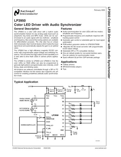
The LP3950 is a color LED driver that can synchronize RGB LEDs to an analog audio input using either amplitude‑ or frequency‑based methods. It is intended for applications such as cellular phones, MP3/CD players, and toys, and can also drive flash LEDs for camera‑phone use.
The device includes a high‑efficiency magnetic DC‑DC boost converter, programmable output voltage, and selectable interfaces (SPI, I²C, or a one‑pin enable line). Detailed pin descriptions, electrical characteristics, and operation modes are provided, along with package information for the 32‑lead thin CSP package.
| Package type | 32‑Lead Thin CSP, 4.5 × 5.5 × 0.8 mm, 0.5 mm pitch |
|---|---|
| Recommended load current | 0 mA to 300 mA |
| Operating voltage range | -0.3 V to +6.0 V |
| Logic input low level | 0.5 V |
| SPI clock frequency | up to 8 MHz |
| I²C clock frequency | up to 400 kHz |
It supports two modes: amplitude‑based and frequency‑based audio synchronization.
The device can be controlled via a 4‑wire SPI interface, a 2‑wire I²C‑compatible interface, or a single‑pin enable line for default operation.
The recommended load current is up to 300 mA.
The package marking includes a date code (XY) and internal codes UZ and TT for die manufacturing and assembly traceability.