
The DAC101C081 is a 10-bit, single channel, voltage-output digital-to-analog converter (DAC) that operates from a +2.7V to 5.5V supply. It has a rail-to-rail output swing and a settling time of 6µs. The DAC101C081 uses the supply voltage as the reference to provide the widest dynamic output range and typically consumes 132µA while operating at 5.0V. It is available in 6-lead TSOT and LLP packages and provides three address options (pin selectable). As an alternative, the DAC101C085 provides nine I2C addressing options and uses an external reference. It has the same performance and settling time as the DAC101C081 and is available in an 8-lead MSOP package. The DAC101C081 and DAC101C085 use a 2-wire, I2C-compatible serial interface that operates in all three speed modes, including high speed mode (3.4MHz). An external address selection pin allows up to three DAC101C081 or nine DAC101C085 devices per 2-wire bus. Pin compatible alternatives to the DAC101C081 are available that provide additional address options. The DAC101C081 and DAC101C085 each have a 16-bit register that controls the mode of operation, the power-down condition, and the output voltage. A power-on reset circuit ensures that the DAC output powers up to zero volts. A power-down feature reduces power consumption to less than a microWatt. Their low power consumption makes them ideal for power-limited applications.
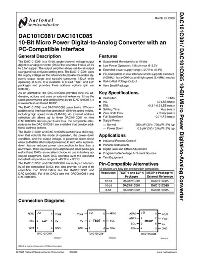
The DAC101C081 and DAC101C085 are 10‑bit, single‑channel, voltage‑output digital‑to‑analog converters that operate from a +2.7 V to 5.5 V supply. They use a 2‑wire I²C‑compatible interface with three speed modes (standard 100 kHz, fast 400 kHz, high‑speed 3.4 MHz) and offer three pin‑selectable address options for the DAC101C081 and nine for the DAC101C085.
The document provides full electrical characteristics, absolute maximum ratings, power‑consumption figures, timing specifications, pin descriptions, ordering information and land‑pattern recommendations. It also includes connection diagrams and notes on usage in industrial temperature ranges from –40 °C to +125 °C.
| Resolution | 10 bits |
|---|---|
| Supply Voltage Range | +2.7 V to +5.5 V |
| Power Consumption (Normal, 3 V) | 380 pW |
| Integral Non‑Linearity (INL) | +2 LSB (max) |
| Differential Non‑Linearity (DNL) | +0.3 / -0.2 LSB (max) |
| Zero Code Error | +10 mV (max) |
| Full‑Scale Error | -0.7 %FS (max) |
The DAC101C081 provides three pin‑selectable address options.
The normal power consumption at 3 V is 380 pW.