
The document describes the features and characteristics of the AT24C1024B product, including low-voltage operation, internal organization, two-wire serial interface, Schmitt triggers, filtered inputs, bidirectional data transfer protocol, different clock rates, hardware and software data protection, page write mode, random and sequential read modes, self-timed write cycle, high reliability, etc.
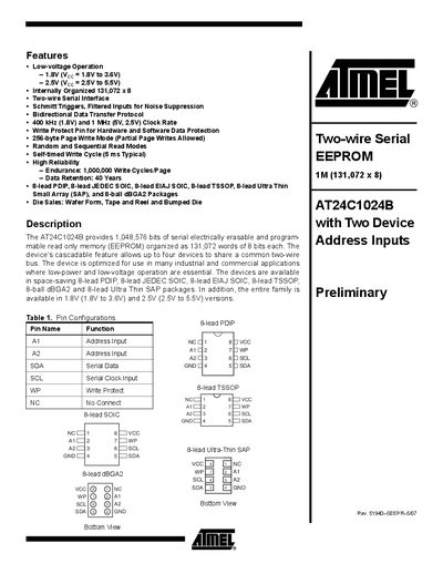
The AT24C1024B provides 1,048,576 bits (131,072 × 8) of serial EEPROM organized in 512 pages of 256 bytes each. It supports low‑voltage operation at 1.8 V (to 3.6 V) or 2.5 V (to 5.5 V) and offers clock rates up to 400 kHz at 1.8 V and 1 MHz at 5 V. The device includes Schmitt‑triggered, filtered inputs, a write‑protect pin, and both hardware and software data protection.
The EEPROM can be cascaded with up to four devices on a common two‑wire bus using the A1/A2 address pins. It features a self‑timed write cycle of about 5 ms, endurance of 1 million write cycles per page, and a data‑retention specification of 40 years. Various 8‑lead and 84‑lead packages are available, and detailed electrical characteristics such as supply voltage, input capacitance, and standby currents are provided in the datasheet.
| Package options | 84‑lead PDIP, 8‑lead JEDEC SOIC, 8‑lead EIAJ SOIC, 8‑lead TSSOP, 8‑lead Ultra Thin SAP, 8‑ball dBGA2 |
|---|---|
| Operating voltage | 1.8 V to 3.6 V (low‑voltage) or 2.5 V to 5.5 V (mid‑voltage) |
| Maximum clock frequency | 400 kHz at 1.8 V, 1 MHz at 5 V |
| Write cycle time | 5 ms typical |
| Endurance | 1,000,000 write cycles per page |
| Data retention | 40 years |
| Input capacitance (SDA) | 8 pF |
The device supports up to 1 MHz clock frequency when operated at 5 V.
Up to four devices can be cascaded on a common two‑wire bus using the A1/A2 address pins.
When WP is tied to GND, normal write operations are allowed; when WP is high, all write operations are inhibited.
A typical write cycle takes about 5 ms.