
This datasheet provides typical application features of LTC2453, including input offset error (INL) and temperature range.
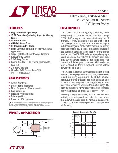
The LTC2453 is a 16‑bit delta‑sigma analog‑to‑digital converter that operates from a single 2.7 V to 5.5 V supply and communicates via a two‑wire I²C bus. It is offered in ultra‑tiny 8‑pin DFN (3 mm × 2 mm) and TSOT‑23 (3 mm × 3 mm) packages and includes an internal oscillator, eliminating the need for external components.
Key features include a proprietary input‑sampling scheme that reduces average input current to ~50 nA, continuous internal offset and full‑scale calibration, auto‑shutdown after each conversion (sleep current <0.2 µA), and a differential input range of ±(VREF+ – VREF–). The device supports up to 60 conversions per second and provides a latency‑free data output.
| Resolution | 16 bits (including sign), no missing codes |
|---|---|
| Supply Voltage (VCC) | 2.7 V to 5.5 V |
| Supply Current (active) | 800 µA typical |
| Sleep Current | < 0.2 µA |
| Conversion Rate | 60 conversions per second |
| I²C Clock Frequency | 0 to 400 kHz |
| Differential Input Range | ±(VREF+ – VREF–) |
| Package Options | 8‑pin DFN (3 mm × 2 mm) or TSOT‑23 (3 mm × 3 mm) |
The LTC2453’s I²C address is hard‑wired to 0010100.
It can perform up to 60 conversions per second.
The sleep current is less than 0.2 µA.
It operates from 2.7 V to 5.5 V.