
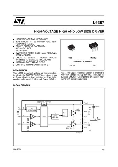
The L6387 is a high‑voltage driver designed with BCD‑OFF‑LINE technology for driving independent N‑channel power MOSFETs on both high‑ and low‑side configurations. It supports a voltage rail up to 600 V and features CMOS/TTL Schmitt‑trigger inputs with hysteresis and pull‑down, as well as an internal bootstrap diode.
The document includes absolute maximum ratings, recommended operating conditions, electrical characteristics, pin descriptions, mechanical dimensions, and a legal disclaimer. It also provides detailed information on the bootstrap driver circuit and input logic behavior.
| Output Voltage Range | -3 V to Vboot - 18 V |
|---|---|
| Floating Supply Voltage (Vboot) | -1 V to 618 V |
| Upper Gate Output Voltage (Vhvg) | 1 V to Vboot |
| Driver Current Capability | 400 mA source, 650 mA sink |
| Switching Times (1 nF load) | Rise 50 ns / Fall 30 ns |
| Total Power Dissipation (Tj = 85 °C) | 750 mW |
| Maximum Junction Temperature | 150 °C |
| Storage Temperature Range | -50 °C to 150 °C |
| Recommended Switching Frequency | 400 kHz |
The output voltage can range from –3 V to Vboot – 18 V.
The recommended switching frequency is 400 kHz when the load capacitance is 1 nF.
It can source 400 mA and sink 650 mA.
The device can dissipate up to 750 mW at a junction temperature of 85 °C.