
The HSP43220 Decimating Digital Filter is a linear phase low pass decimation filter which is optimized for filtering narrow band signals in a broad spectrum of a signal processing applications. The HSP43220 offers a single chip solution to signal processing applications which have historically required several boards of ICs. This reduction in component count results in faster development times as well as reduction of hardware costs. The HSP43220 is implemented as a two stage filter structure. As seen in the block diagram, the first stage is a high order decimation filter (HDF) which utilizes an efficient sample rate reduction technique to obtain decimation up to 1024 through a coarse low-pass filtering process. The HDF provides up to 96dB aliasing rejection in the signal pass band. The second stage consists of a finite impulse response (FIR) decimation filter structured as a transversal FIR filter with up to 512 symmetric taps which can implement filters with sharp transition regions. The FIR can perform further decimation by up to 16 if required while preserving the 96dB aliasing attenuation obtained by the HDF. The combined total decimation capability is 16,384. The HSP43220 accepts 16-bit parallel data in 2’s complement format at sampling rates up to 33MSPS. It provides a 16-bit microprocessor compatible interface to simplify the task of programming and three-state outputs to allow the connection of several ICs to a common bus. The HSP43220 has low power consumption and operates over a wide supply voltage range of 1.8V to 3.3V and does not require an external clock.
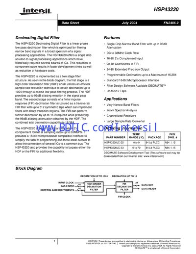
The HSP43220 is a linear‑phase decimating digital filter integrated in a single chip, offering a high‑order low‑pass filter with up to 96 dB alias rejection for narrow‑band signal processing.
It features a 16‑bit 2’s‑complement input, 24‑bit extended‑precision output, programmable decimation up to 16,384, and up to 512 symmetric FIR taps, with a maximum clock rate of 33 MHz. The device includes a high‑order decimation filter stage, a FIR stage, and control registers accessible via a standard 16‑bit microprocessor interface.
| Maximum clock rate | 33 MHz |
|---|---|
| Maximum clock frequency (CK_IN / FIR_CK) | 33 MHz |
| Output precision | 24‑bit extended |
| Input data format | 16‑bit 2’s complement |
| Alias rejection | up to 96 dB |
| Maximum decimation factor | 16,384 |
| Maximum FIR taps | 512 symmetric taps |
The device operates with a maximum clock frequency of 33 MHz.
The filter can be programmed with up to 512 symmetric FIR taps.
It offers up to 96 dB of aliasing rejection in the low‑pass decimation filter.
The input data is a 16‑bit 2’s‑complement fractional format.