
ISL65426MREP is a high efficiency dual output monolithic synchronous buck converter operating over an input voltage range of 2.5V to 5.5V. This single chip power solution provides two output voltages which are selectable or externally adjustable from 1.2V to 80% of the supply voltage while delivering up to 6.0A of total combined output current when used at TJ of +125°C or less. The two PWMs are synchronized 180° out of phase reducing the RMS input current and ripple voltage. The ISL65426MREP switches at a fixed frequency of 1MHz and utilizes current-mode control with integrated compensation to minimize the size and number of external components. The internal synchronous power switches are optimized for good thermal performance, high efficiency, and eliminate the need for an external Schottky diode. A unique power block architecture allows partitioning to support one of four configuration options. One master power block is associated with each synchronous converter channel. Four floating slave power blocks allow the user to assign them to either channel. Proper external configuration of the power blocks is verified internally prior to soft-start initialization. Independent enable inputs allow for synchronization or sequencing soft-start intervals of the two converter channels. A third enable input allows additional sequencing for multi-input bias supply designs. Individual p
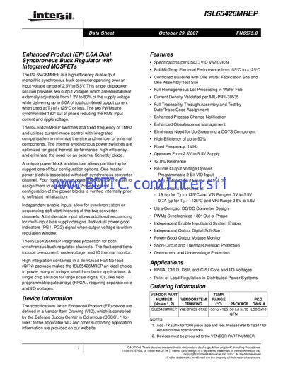
The ISL65426MREP is a high‑efficiency dual‑output monolithic synchronous buck converter that operates from 2.5 V to 5.5 V input and provides selectable output voltages. It delivers up to 6.0 A of combined output current while maintaining up to 90 % efficiency and operates over a temperature range of –55 °C to +125 °C.
Key features include 1 MHz fixed‑frequency operation, synchronized 180° out‑of‑phase PWM channels, independent enable inputs, power‑good indicators, and integrated over‑current, undervoltage, and thermal‑overload protection. The device is offered in a thin 50‑lead QFN package suitable for compact, high‑density designs such as FPGA, CPLD, DSP, and CPU core/I‑O voltage regulation.
| Input voltage range | 2.5 V to 5.5 V |
|---|---|
| Maximum combined output current | 6.0 A |
| Switching frequency | 1 MHz (fixed) |
| Efficiency | up to 90 % |
| Operating temperature range | -55 °C to +125 °C |
| Package | 50‑lead QFN |
| Typical current (VIN 4.0‑5.5 V) | 1 A |
| Typical current (VIN 2.5‑5.5 V) | 0.7 A |
The device operates from 2.5 V to 5.5 V supply.
It can deliver up to 6.0 A of total combined output current.
The regulator includes short‑circuit, over‑current, undervoltage, and thermal‑overload protection.
The converter switches at a fixed frequency of 1 MHz.