
This document describes the features and characteristics of a high-performance, low-power AVR® 8-bit microcontroller. It utilizes an advanced RISC architecture with 131 powerful instructions, most of which can be executed in a single clock cycle. It also features 32 x 8 general purpose working registers, fully static operation, and an on-chip 2-cycle multiplier. The microcontroller includes high endurance non-volatile memory segments, such as in-system self-programmable flash program memory, EEPROM, and internal SRAM. It supports in-system programming by an on-chip boot program and true read-while-write operation. The microcontroller also provides JTAG interface with boundary-scan capabilities, extensive on-chip debug support, and the ability to program flash, EEPROM, fuses, and lock bits through the JTAG interface. Additionally, it offers various peripheral features including timers/counters, PWM channels, ADC differential mode, serial interfaces, and more.
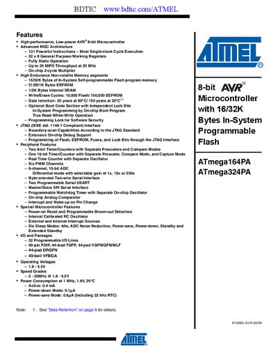
The ATmega324PA is a low‑power 8‑bit CMOS microcontroller based on Atmel's enhanced AVR RISC architecture. It delivers up to 20 MIPS at 20 MHz and includes a rich set of peripherals such as timers, ADC, USARTs, SPI, and JTAG.
The document details the device's features, pin‑out diagrams for various packages, memory organization, electrical characteristics, power‑saving modes, and revision history, allowing designers to integrate the microcontroller into embedded applications.
| Flash program memory | 32 Kbyte |
|---|---|
| EEPROM | 1 Kbyte |
| SRAM | 2 Kbyte |
| Maximum clock speed | 20 MHz |
| Active power consumption (1 MHz, 1.8 V) | 0.4 mA |
| Package options | 40‑pin PDIP, 44‑lead TQFP, 44‑pad VQFN/QFN/MLF, 44‑pad DRQFN, 49‑ball VFBGA |
The ATmega324PA provides 32 Kbyte of In‑System Self‑Programmable Flash memory.
It is offered in 40‑pin PDIP, 44‑lead TQFP, 44‑pad VQFN/QFN/MLF, 44‑pad DRQFN, and 49‑ball VFBGA packages.
It consumes about 0.4 mA in active mode under those conditions.