
The AD8159 Rev. A is a 3.2 Gbps quad buffer multiplexer/demultiplexer with port-level 2:1 mux/1:2 demux functionality. Each port consists of 4 lanes, with each lane running from dc to 3.2 Gbps independently. It compensates for over 40 inches of FR4 at 3.2 Gbps through two levels of input equalization or four levels of output pre-emphasis. The product accepts ac- or dc-coupled differential CML inputs and has low deterministic jitter, low random jitter, and a BER of less than 10^-16. It also features on-chip termination, reversible inputs and outputs on one port, unicast or bicast on the 1:2 demux function, port-level loopback capability, and single lane switching capability. The AD8159 operates on a 3.3 V core supply and has a flexible I/O supply down to 2.5 V. It is a low power device, typically consuming 1 W in the basic configuration. The operating temperature range is -40°C to +85°C. The AD8159 is suitable for applications such as low-cost redundancy switches and SONET OC48/SDH16 and lower data rates.
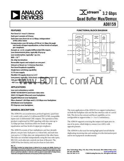
The AD8159 is an asynchronous, protocol‑agnostic quad‑lane 2:1 switch with 12 differential inputs and 12 differential outputs. Each lane operates independently up to 3.2 Gbps and offers two levels of input equalization and four levels of output pre‑emphasis, providing low deterministic jitter (20 ps p‑p) and low random jitter (1 ps rms).
Typical applications include low‑cost redundancy switching for backplane links such as SONET OC48/SDH16, XAUI, Gigabit Ethernet, Fibre Channel, Infiniband, and PCI‑Express. The device also supports unicast/bicast operation, reversible ports, and loopback for testing high‑speed serial links.
| Data Rate/Channel (NRZ) | 3.2 Gbps |
|---|---|
| Propagation Delay (input to output) | 600 ps |
| Lane‑to‑Lane Skew | 100 ps |
| Switching Time | 5 ns |
| Output Rise/Fall Time (20%‑80%) | 100 ps |
| Input Bias Current | 4 pA |
| Core Supply Voltage (VEE) | 3.0‑3.6 V |
| Operating Temperature Range | -40 °C to +85 °C |
Each lane supports up to 3.2 Gbps.
The core supply voltage must be between 3.0 V and 3.6 V.