
This document describes the features and characteristics of the AD8156, a 6.25 Gbps, 4×4 digital crosspoint switch. The switch supports dual 2×2 operation, with a data rate of up to 6.25 Gbps per channel. It features programmable input equalization to compensate for over 40 inches of FR-4 material at 6.25 Gbps. The switch supports multicast and broadcast modes of operation, and has programmable output swing. It operates at a power supply voltage of 3.3 V (±10%), with low power consumption. The inputs can be AC-coupled or DC-coupled, and support a wide range of DC-coupled input standards. The control is LVTTL- or LVCMOS-compatible. The switch has low additive jitter and low random jitter characteristics.
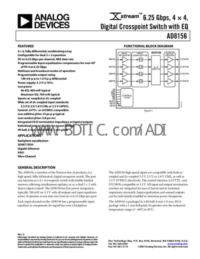
The AD8156 is a high‑speed, fully differential digital crosspoint switch from Analog Devices. It can operate as a 4 × 4 switch with double‑latched memory or as dual 2 × 2, offering programmable input equalization, multicast/broadcast modes, and LVTTL/LVCMOS‑compatible control.
Packaged in a 49‑ball CSP‑BGA (8 mm × 8 mm) and rated for –40 °C to 85 °C, the device runs from a 3.3 V supply and dissipates as little as 60 mW (all disabled) up to about 700 mW when fully active. It targets backplane equalization, SONET/SDH, Gigabit Ethernet, XAUI, and Fibre Channel applications.
| Maximum Data Rate | 6.25 Gbps |
|---|---|
| Supply Voltage | 3.3 V (±10%) |
| Typical Power Dissipation (all active) | 700 mW |
| Input Voltage Swing | 200‑2000 mV p‑p |
| Output Voltage Swing (programmable) | 50‑1850 mV p‑p |
| Operating Temperature Range | -40 °C to 85 °C |
The AD8156 supports up to 6.25 Gbps NRZ data rate.
It operates from a 3.3 V supply (±10%).
The device is packaged in a 49‑ball CSP‑BGA (8 mm × 8 mm).
Typical power dissipation is about 700 mW.