
The ADP5033 is a dual 3 MHz, 800 mA buck regulator with two 300 mA LDOs in a tiny, 16-ball, 2 mm × 2 mm WLCSP package. It is designed to meet demanding performance and board space requirements. Applications include power for processors, ASICS, FPGAs, and RF chipsets, portable instrumentation and medical devices.
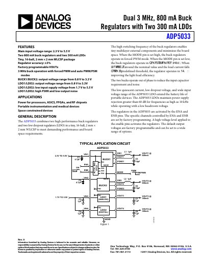
The ADP5033 combines two high‑performance 800 mA buck regulators and two low‑dropout 300 mA LDOs in a tiny 16‑ball 2 mm × 2 mm wafer‑level chip‑scale package. It operates from a wide input range and offers ±3 % voltage accuracy, with both forced PWM and auto PWM/PSM modes.
The document provides full electrical specifications, pin configuration, thermal data, recommended external components, and typical application circuits for processor, ASIC, FPGA and RF chipset power supplies. Ordering information and package dimensions are also included.
| Input voltage range (VIN1/VIN2) | 2.3 V to 5.5 V |
|---|---|
| Input voltage range (VIN3/VIN4) | 1.7 V to 5.5 V |
| Buck regulator output voltage range | 0.8 V to 3.3 V |
| LDO output voltage range | 0.8 V to 3.3 V |
| Switching frequency | 3 MHz |
| Regulator accuracy | ±3 % |
| Package | 16‑ball 2 mm × 2 mm WLCSP |
| Operating temperature range (TJ) | −40 °C to +125 °C |
| Quiescent current (all channels enabled, no load) | 108 µA (typ) |
It contains two 800 mA buck regulators and two 300 mA low‑dropout regulators.
The buck regulators operate at a switching frequency of 3 MHz.
The device is offered in a 16‑ball 2 mm × 2 mm wafer‑level chip‑scale package (WLCSP).