
The AD7740 is a low-cost, ultrasmall synchronous voltage-to-frequency converter (VFC). It works from a single 3.0 V to 3.6 V or 4.75 V to 5.25 V supply consuming 0.9 mA. The AD7740 is available in an 8-lead SOT-23 and also in an 8-lead microSOIC package. Small package, low cost and ease of use were major design goals for this product. The part contains an on-chip 2.5 V bandgap reference but the user may overdrive this using an external reference.
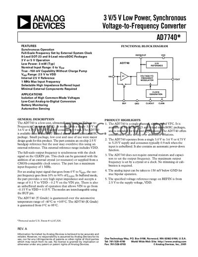
The AD7740 is a low‑cost, ultra‑small voltage‑to‑frequency converter (VFC) that operates from a single 3.0 V‑3.6 V or 4.75 V‑5.25 V supply. It features a synchronous design, an on‑chip 2.5 V bandgap reference, and selectable buffered or unbuffered input modes, allowing input ranges from –0.15 V to VDD + 0.15 V (unbuffered) or 0.1 V to VDD – 0.2 V (buffered). The device supports a maximum input frequency of 1 MHz and provides a frequency output proportional to the analog input.
Typical applications include isolation of high common‑mode voltages, low‑cost analog‑to‑digital conversion, battery monitoring, and automotive sensing. The datasheet includes detailed pin configurations, timing characteristics, absolute maximum ratings, and example circuits such as temperature‑sensor integration and crystal‑based clock generation.
| Supply Voltage Range | 3.0 V‑3.6 V or 4.75 V‑5.25 V |
|---|---|
| Typical Power Consumption (Unbuffered) | 0.9 mA |
| Maximum Input Frequency | 1 MHz |
| Reference Voltage Range | 2.5 V to VDD |
| Power‑Down Current (Typical) | 100 pA |
It operates from a single 3.0 V‑3.6 V or 4.75 V‑5.25 V supply.
When the CLKIN input is inactive low for 1 ms, the device automatically enters power‑down, reducing consumption to about 525 µW at 5 V.
The device supports input frequencies up to 1 MHz.
The K version is guaranteed from 0 °C to 85 °C, while the Y version operates from –40 °C to +105 °C.