
The document introduces the AD8330 variable gain amplifier, which has the characteristics of low cost, low noise, low distortion, and low power consumption. It is suitable for applications such as pre-ADC signal conditioning, 75Ω cable driving, etc.
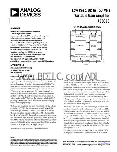
The AD8330 is a low‑cost, DC‑to‑150 MHz variable gain amplifier with a fully differential signal path that can also accept single‑ended inputs. It offers programmable gain from 0 dB to 50 dB, low noise (5 nV/√Hz), low distortion (<‑62 dBc), and constant 150 MHz bandwidth across the gain range.
The datasheet provides a functional block diagram, detailed specifications, absolute maximum ratings, pin descriptions for both LFCSP and QSOP packages, typical performance graphs, and application notes such as pre‑ADC conditioning and AGC amplifier designs.
| Supply Voltage | 6 V |
|---|---|
| Operating Temperature Range | -40°C to +85°C |
| Quiescent Current | 20 mA typical |
| Small‑Signal -3 dB Bandwidth | 150 MHz |
| Peak Slew Rate | 1500 V/µs |
| Input Resistance (typical) | 1 kΩ |
| Input Capacitance | 4 pF |
| Voltage Noise Spectral Density | 5 nV/√Hz |
| Peak‑to‑Peak Output Swing | 2 V |
| Common‑Mode Voltage (typical) | 2.5 V |
The gain can be programmed from 0 dB to 50 dB using the VDBS control pin, with a slope of 30 mV per dB.
The device provides a constant 150 MHz bandwidth at all gain settings.
The AD8330 operates from a 6 V supply and draws about 20 mA typical quiescent current at 5 V.
It is offered in 16‑lead LFCSP and 16‑lead QSOP packages.