
QFN-20 Power Dissipation Datasheet, including measurement conditions and power dissipation vs. ambient temperature
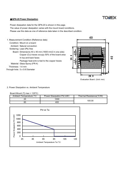
This datasheet presents measured power‑dissipation values for the QFN‑20 package. The data are intended as reference for designers evaluating thermal performance under the described conditions.
Measurements were taken with the package mounted on a 40 × 40 mm board (1600 mm² per side), natural convection, lead‑free soldering, FR‑4 substrate (1.6 mm thick), copper traces covering 50 % of the board area, and a through‑hole of 5 × 0.8 mm. The table shows power dissipation versus ambient temperature and the thermal resistance of 100 °C/W, with a maximum junction temperature of 125 °C.
| Package dimensions | 40 × 40 mm (1600 mm² per side) |
|---|---|
| Copper trace coverage | 50 % of board area |
| Substrate material | Glass Epoxy (FR‑4) |
| Substrate thickness | 1.6 mm |
| Through‑hole size | 5 × 0.8 mm |
| Maximum junction temperature | 125 °C |
The maximum junction temperature (Tj max) is 125 °C.