
S3C44B0X is a ARM7TDMI core processor
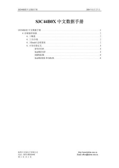
The S3C44B0X datasheet provides a detailed description of the internal memory controller, which supplies two sets of control signals for external memory operations. It outlines the selectable endian mode, address space per bank, and programmable bus widths for each of the eight memory banks.
The document also defines the BWSCON and BANKCON registers that configure bus width, wait states, and timing parameters for ROM, SRAM, and DRAM/SDRAM banks, as well as the REFRESH register that controls DRAM refresh modes and timing. This manual is written in Chinese.
| Address space per bank | 32M bytes |
|---|---|
| Total number of memory banks | 8 |
| Programmable bus width | 8/16/32 bits |
The device provides eight memory banks.
Bus width is set via the BWSCON register for most banks and via the OM[1:0] pins for the BOOT ROM bank.