
74LVXC3245 8-Bit Dual Supply Configurable Voltage Interface Transceiver with 3-STATE Outputs
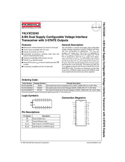
The 74LVXC3245 is a 24‑pin dual‑supply, 8‑bit configurable voltage interface transceiver designed for PCMCIA and other real‑time I/O applications. It supports bidirectional communication between 3 V and 3 V‑to‑5 V buses, with 3‑STATE outputs that can source or sink up to 24 mA.
The document provides detailed electrical characteristics, absolute maximum ratings, recommended operating conditions, package information, and power‑up sequencing guidelines. It also includes mechanical dimensions, ordering codes, and compliance notes such as the life‑support policy.
| Supply voltage Voca range | 2.7 V to 3.6 V |
|---|---|
| Supply voltage Vcp range | 3.0 V to 5.5 V |
| Output source/sink current | up to 24 mA |
| Input capacitance (CIN) | 45 pF |
| Output capacitance (COUT) | 10 pF |
| Typical propagation delay (Voca=3.3 V, Voce=5.0 V) | 1.0 ns (typ) |
| Quiescent power consumption | < 1 mW |
The transceiver can source or sink up to 24 mA per output pin.
Voca is recommended between 2.7 V and 3.6 V, while Vcp should be between 3.0 V and 5.5 V.
Power the Voca side first, ramp OE with or ahead of Voca, and ramp the T/R pin with Vcp so that the A‑Port pins are configured as inputs during power‑up.