
This datasheet introduces the features of PIC24FJ64GA004 series microcontrollers, including CPU, memory, analog characteristics, peripheral characteristics, etc.
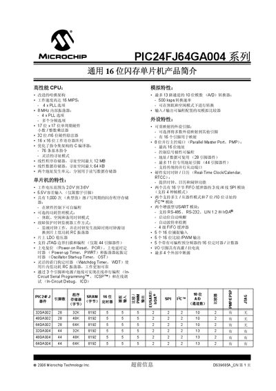
The PIC24FJ64GA004 is a 16‑bit flash microcontroller offering up to 16 MIPS CPU performance, 2.0 V‑3.6 V operating voltage, and on‑chip peripherals such as a 13‑channel 10‑bit ADC, enhanced USART, PWM, real‑time clock/calendar, and an on‑chip LDO regulator. It supports multiple power‑saving modes and JTAG boundary‑scan for development.
The manual includes detailed pin‑out tables for 28‑pin PDIP/SOIC, 44‑pin QFN and TQFP packages, electrical characteristics, memory organization (up to 12 MB flash and 64 KB RAM), and usage guidelines for the device’s peripherals and programming interfaces. This manual is written in Chinese.
| CPU speed | 16 MIPS |
|---|---|
| Operating voltage | 2.0 V to 3.6 V |
| Flash program memory | up to 12 MB |
| Data RAM | up to 64 KB |
| ADC channels | 13 channels, 10‑bit, 500 ksps |
| Internal oscillator | 8 MHz with 4× PLL |
| On‑chip LDO regulator | present |
| JTAG support | boundary‑scan supported |
| Real‑Time Clock/Calendar | time, date, week functions |
| PWM resolution | 16‑bit |
The device operates from 2.0 V up to 3.6 V.
It can hold up to 12 MB of flash program memory.
The microcontroller offers up to 13 channels of 10‑bit ADC with a conversion rate of 500 ksps.
Yes, it supports JTAG boundary‑scan debugging.